- DIY
- A
Used Antminer S9 for amateur radio enthusiasts. Part II
Continuing from the previous article, I will talk about using the Antminer S9 to create a sequencer for the transceiver. Here, there will be more mindful use of FPGA, creating a custom IP block in Verilog, simulation, and other useful things for a beginner Antminer S9 user. If you're interested, please read on.
For those who are hearing the word sequencer in relation to radio for the first time, here's a brief introduction. To operate a transceiver, you need a receiver-transmitter and an antenna connected by a cable. The cable can be quite long, and there are significant losses in the useful signal, which increase with the signal frequency. Therefore, additional amplifiers are installed near the antenna in the VHF and higher frequency bands to compensate for these losses. However, another problem arises: typically, the same antenna is used for both receiving and transmitting. So, at the moment of transmission, you need to connect a power amplifier (PA) to the antenna, and at the moment of receiving, you connect a low-noise amplifier (LNA). Switching is usually done using powerful relays, whose response time is in the tens of milliseconds. During switching, a situation can occur where, for example, the transceiver's transmitter is still on, and the LNA is still connected to the antenna. In this case, the powerful signal from the transmitter can damage the LNA.
The solution to this situation is to add a delay between switching the receive/transmit relay and turning on the transmitter. This work is done by a device called a sequencer.
This is a rather simple device, which radio enthusiasts have been making themselves for decades. The simplest versions can be made just with a couple of relays, as shown, for example, in this diagram.

As technology has progressed, radio enthusiasts have made sequencers using many methods: transistors, comparators, timers. Recent developments increasingly use microcontrollers. I decided to go further and make a sequencer on an FPGA.
Here is a typical schematic recommended by US4ICI for their LNAs and sequencers (https://vhfdesign.com/ru/other/sequencer-pcb.html):

The picture shows the timing diagram of the sequencer's operation, ensuring the sequential turning on and off of devices when switching to transmit mode and back.
One might ask: why make your own sequencer, especially on an FPGA, when you can simply make one with relays or buy a ready-made board?
First, it's just interesting to use new technologies to solve everyday tasks, and it's not too expensive thanks to the current price of a used Antminer S9 board (300-$7.69).
Secondly, I'll try to explain rationally:
I need a sequencer for working through amateur radio satellites. This uses duplex mode on separated frequencies. So, if an antenna and LNA are used for receiving on the 70 cm band (U band), then for transmission, an antenna and PA are needed for the 2m band (V band). And all of this works simultaneously, also using two feeders. When switching between satellites, the combination of satellite frequency ranges used (V/U, U/V, U/U, V/V) can change. It can be seen that switching in this case is much more complicated than working in one band in half-duplex mode.

From the previous article, you could learn that I have difficulties with laying cables on the roof. And here I demonstrate frugality. Thus, for each range, I use only one wire to control the activation of the MSHU or UM. This is done simply:
If no voltage is applied to the wire, the antenna is directly connected to the feeder.
If 12 volts are applied to the wire, the MSHU will be connected to the antenna on the roof.
If 36 volts are applied to the wire, the UM will be connected to the antenna instead of the MSHU. The 36-volt voltage is relatively safe and helps reduce current through the wires when the UM is operating. The UMs are made on MITSUBISHI modules and powered by DC-DC converters from 36V to 13.8V.
I want the sequencer to automatically adjust to the selected reception and transmission ranges. This is exactly why I modified the LibreSDR firmware, as I wrote in this article (https://habr.com/ru/articles/880926/). If you look, you will see that the LibreSDR band data is output via UART to transmit information about the current transmission and reception frequencies. This data should go to the sequencer and automatically determine the switching logic when changing reception and transmission modes.
In my transceiver design, there are several protection circuits for the UM: from current overload, SWR, and power. I created a hardware protection circuit for exceeding the set limits for these parameters. This circuit forms a logical FAULT signal that notifies the sequencer of an emergency situation. In turn, the sequencer must react as quickly as possible and disconnect everything in an attempt to prevent the development of an accident. It is better to implement this logic in hardware rather than software. It will work faster and more reliably. Therefore, this is the perfect place to use FPGA.
The hardware sequencer itself, in my opinion, should have greater reliability than the software one. Ideally, it should not be sensitive to possible failures and errors in the control program.
As you can see, this is quite an original solution with specific requirements, and there is no ready-made switching diagram for it, so something of my own needs to be invented. It's just the right time to try using an Antminer S9.
Armed with textbooks on Verilog, we begin writing the sequencer code. First, I wrote the code for the sequencer to work only with the 2-meter range. It looks like a typical Finite State Machine (FSM). FSM (Finite State Machine) is a mathematical model used to describe the behavior of systems that can be in one of a finite number of states and transition between them in response to events. Finite State Machines are very convenient for writing Verilog code. The result is clear code with understandable logic.
At the beginning of the code, the input and output signals of the sequencer are defined:
module seq144 #
	(
        parameter integer SEQ_DELAY = 1500000
	)
(
  input clk, // Clock input signal
  input reset, // Asynchronous reset input signal
  input ptt, // Push-to-talk input signal. 0 is active
  output reg lna144, // LNA enable output signal
  output reg pa144, // Lower PA enable output signal
  output reg a144 // Pre-amplifier, relay, upper PA enable output signal
);

// Possible FSM states
localparam READY_STATE 				= 4'b0001;	// 1
localparam TRANSMIT_START_STATE		= 4'b0010;	// 2
localparam TRANSMIT_START2_STATE 	= 4'b0100;	// 4
localparam TRANSMIT_STATE			= 4'b1000;	// 8

reg        [3:0] State;
reg        [3:0] NextState;
It is clear that the clock and reset signals need to be considered for the machine to initialize to the correct state. The list of possible states is also defined here.
Next, it describes how the time delay between state transitions will be managed. Delays are implemented by creating a counter register for the clock signal. A countdown is performed. In my case, the clock frequency is 50 MHz, and the counter should count from 1500000 down to 0 before transitioning to the next state. The counter is reset on the reset signal.
parameter DELAY_CNT_SIZE = 21;
reg [DELAY_CNT_SIZE - 1 : 0] DCounter;

// Delay counter processing
always @(posedge clk)
  begin
    if(reset)
      begin
        DCounter <= 0;
      end
    else
      begin
        // The counter counts down to 0, except
        // during state changes, when the delay for the next state is set

		// DELAY_SETUP
		if(ptt == 1'b0) // transmission enabled
			begin
				if ((State == READY_STATE) && (NextState == TRANSMIT_START_STATE))
					DCounter <= SEQ_DELAY;
				else if((State == TRANSMIT_START_STATE) && (NextState == TRANSMIT_START2_STATE))
					DCounter <= SEQ_DELAY;
			end
		else // transmission disabled
			begin
				if ((State == TRANSMIT_STATE) && (NextState == TRANSMIT_START2_STATE))
					DCounter <= SEQ_DELAY;
				else if((State == TRANSMIT_START2_STATE) && (NextState == TRANSMIT_START_STATE))
					DCounter <= SEQ_DELAY;
			end
        //----------------------------------------------------------
        if(DCounter != 0)
		begin
          DCounter <= DCounter - 1'b1;
		end
	  end
  end
The state machine is divided into two parts. The first part is responsible for generating output signals based on the FSM state:
always @(posedge clk)
  begin
    if(reset)
      begin
        lna144 <= 1'b1;
        a144   <= 1'b0;
        pa144  <= 1'b0;
      end
    else
      begin
        // To ensure the output value changes along with the state change,
        // and not on the next clock cycle, NextState is analyzed
        case(NextState)
          READY_STATE:
            begin
			  lna144 <= 1'b1;
			  a144   <= 1'b0;
			  pa144  <= 1'b0;
            end
          TRANSMIT_START_STATE:
            begin
			  lna144 <= 1'b0;
			  a144   <= 1'b0;
			  pa144  <= 1'b0;
            end
          TRANSMIT_START2_STATE:
            begin
			  lna144 <= 1'b0;
			  a144   <= 1'b1;
			  pa144  <= 1'b0;
            end
          TRANSMIT_STATE:
            begin
			  lna144 <= 1'b0;
			  a144   <= 1'b1;
			  pa144  <= 1'b1;
            end
        endcase
      end
  end
The second part is responsible for performing state transitions:
always @(*)
  begin
    //by default save the current state
    NextState = State;

    case(State)
      //--------------------------------------
      READY_STATE:
        begin
          if(ptt == 1'b0) //transmission is enabled
            begin
              NextState = TRANSMIT_START_STATE;
            end
        end

      //--------------------------------------
      TRANSMIT_START_STATE:
        begin
          if ((DCounter == 0) && (ptt == 1'b0))
            begin
              NextState = TRANSMIT_START2_STATE;
            end
		  else if ((DCounter == 0) && (ptt == 1'b1))
            begin
              NextState = READY_STATE;
            end
        end

      //--------------------------------------
      TRANSMIT_START2_STATE:
        begin
          if ((DCounter == 0) && (ptt == 1'b0))
            begin
              NextState = TRANSMIT_STATE;
            end
		  else if ((DCounter == 0) && (ptt == 1'b1))
            begin
              NextState = TRANSMIT_START_STATE;
            end
        end

      //--------------------------------------
      TRANSMIT_STATE:
        begin
          if(ptt == 1'b1) //transmission is disabled
            begin
              NextState = TRANSMIT_START2_STATE;
            end
        end
      //--------------------------------------
      default: NextState = READY_STATE;
    endcase
  end
Everything looks good in the final form, but it did not work right away. Therefore, I find it necessary to mention the mandatory need to run the circuit simulation in a simulator. One should not neglect writing tests for circuit code.
For simulation in Vivado, there is a separate section, as it is obvious, called SIMULATION. In the "sources" section, there is a folder named Simulation sources. To perform the simulation, you need to write a so-called test bench file. It is written in the same Verilog, but with additional syntactic constructs for testing purposes. For my sequencer, I wrote such a test:
module seq144_tb;
   //Inputs in the module seq144. Need to use register type
	reg clk = 0;
	reg rst = 0;
	reg ptt = 1;
	//Outputs in the module seq144. Need to use net type
   wire lna144;
   wire pa144;
   wire a144;
	// Instantiate the Unit Under Test (UUT) for module
	seq144 uut (
		.clk(clk),
		.reset(rst),
		.ptt(ptt),
		.lna144(lna144),
		.pa144(pa144),
		.a144(a144)
	);

   // Generate the continuous clock signal. Wait for 10ns. Period is 20ns
   always #10 clk = ~clk;

	initial
	begin
	   rst = 1;
	   #40
	   rst = 0;
	   #40
	   ptt = 0;
	   #200
	   ptt = 1;
	   #180
	   ptt = 0;
	   #500
	   $finish();
	end

endmodule
As you can see, the test initializes the sequencer module, the clock signal, and during the test, the input signal values change at intervals in nanoseconds (#40 means waiting 40 ns). The test ends with the $finish() instruction.
This is only the test code. To run it, you need to make the module the top in the test list, i.e., execute the "Set as top" command in the Vivado menu. In this case, when you start the simulation, the test will begin with this module.
Next, we run the simulation and get some result, for example:
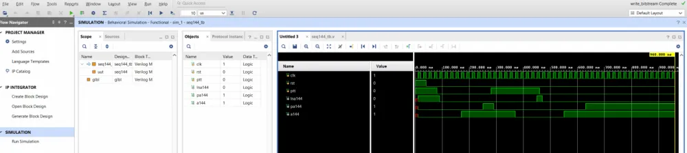
You can see how the logic levels of the signals change over time while the sequencer module is running. Carefully examine and modify your code if there is any logic violation.
You can debug not in the simulator, but in the ready-made system. Then, you need to add an ILA module to the design. Its description goes beyond the scope of this article.
The sequencer module is written, but I wanted it to automatically configure itself depending on the selected frequency ranges of the transceiver. This can be done in different ways, but I chose configuration through a program-controlled write to the operational memory of the sequencer's configuration settings.
To organize such a working mode in Vivado, there is a rather complex path. It is necessary to create your own IP block with an interface to the AXI4 bus. Vivado will automatically set up the connection to the bus and provide an address in the system's general address space for the block to work. At this address, the application program will need to write the sequencer configuration.

In the Vivado menu, there is the Tools->Create and package new IP item. When invoked, a wizard appears where you need to select Create new AXI4 peripheral. Then the wizard will generate all the necessary wrapper code required to connect the block to the AXI bus. The code will indicate places where the user should add their functionality. Here is what I came up with:

I had to go this route, add a sequencer call to the new IP module code, and link the sequencer configuration registers with the AXI bus registers.
The hints in the template code are clear. It is clear how to use the registers that the control program writes. But how to write a register to the bus from your Verilog code is not very clear. At least, the template does not provide for such usage, but I did it so that the sequencer state would be written to the second register:
assign slv_reg_rden = axi_arready & S_AXI_ARVALID & ~axi_rvalid;
	always @(*)
	begin
	      // Address decoding for reading registers
	      case ( axi_araddr[ADDR_LSB+OPT_MEM_ADDR_BITS:ADDR_LSB] )
	        2'h0   : reg_data_out <= slv_reg0;
	        2'h1   : reg_data_out <= { 21'b0, lna144, a144, pa144, lna430, a430, pa430, slv_reg0[2:0], hard_fault, ptt};
	        //2'h1   : reg_data_out <= slv_reg1;
	        2'h2   : reg_data_out <= slv_reg2;
	        2'h3   : reg_data_out <= slv_reg3;
	        default : reg_data_out <= 0;
	      endcase
	end
The finished block is embedded in the overall sequencer scheme. The full diagram looks like this:

You can see how the sequencer block is embedded in the diagram. Also, the hard logic for processing the FAULT alarm signal is visible.
A few words about accessing memory and the AXI bus from the control program. In general, the Linux OS blocks direct memory access for users. Proper design involves writing a kernel module, from which such access is possible. But I did not want to write a kernel module. For lazy people like me, there is a workaround. Linux can be configured so that a /dev/mem device appears. In the kernel build config, you need to write:
CONFIG_DEVMEM=y
With root privileges, you can directly read and write to memory using this device. The devmem and devmem2 utilities allow you to access memory from the Linux command line, which is convenient for debugging.
For working with such memory, there is a Rust crate called ddevmem. An example of its use for reading and writing to memory:
use ddevmem::{register_map, DevMem};

register_map! {
    pub unsafe map MyRegisterMap {
        0x00 => rw reg0: u32,
        0x04 => ro reg1: u32,
        0x08 => wo reg2: u32
    }
}

let devmem = unsafe { DevMem::new(0xD0DE_0000, None).unwrap() };
let mut reg_map = unsafe { MyRegisterMap::new(std::sync::Arc::new(devmem)).unwrap() };
let (reg0_address, reg0_offset) = (reg_map.reg0_address(), reg_map.reg0_offset());
let reg1_value = *reg_map.reg1();
*reg_map.reg2_mut() = reg1_value;
The control program for my sequencer is written in Rust. It receives data from LibreSDR over UART about the current receiving and transmitting ranges, then writes the configuration using devmem to the sequencer registers.
Retreat on bugs. To build the project, as usual, you need to generate the bitstream and create the FSBL. At this stage, after creating my IP block, I encountered a problem. Vivado generates an XSA description file, based on which the FSBL is created. This file is just a ZIP archive, and if you look inside, you will find, for example, the makefile for building Zynq boot code. So, the automatically created FSBL project refused to compile the automatically created Vivado code. The problem turned out to be in the generated makefile for building the IP. I had to replace it with a similar file from the uartlite IP block, after which the FSBL compiled without problems. Perhaps this is just a bug in Vitis 2022, and there are no such problems in newer versions.
Additionally, I decided to display all system status information on an SPI LCD screen. When the screen appeared, I wanted to display additional information about transmission power and VSWR on it.

I added the ADC module ADS1115 to the system. This turned the sequencer from a utilitarian functional block into the control center for the transceiver, monitoring its operation.
During the use of the Antminer S9, I discovered one unpleasant feature. Until the system has booted, the FPGA outputs may have undefined signal levels. For this reason, the relays connected to the FPGA could randomly turn on when the system was powered on, which was an unacceptable behavior. I had to add a block to the design that would supply power to the relay switching block only after the system had fully booted and the control program had started.
For this purpose, I used the DAC module mcp4725.

When the power is turned on, its output guarantees 0 volts. I connected the DAC output to the key transistor for powering the relay switching block. At the start of the control program, it sets the DAC output to 5 V over the I2C bus, which powers the system. Thus, the undefined behavior at startup was eliminated.
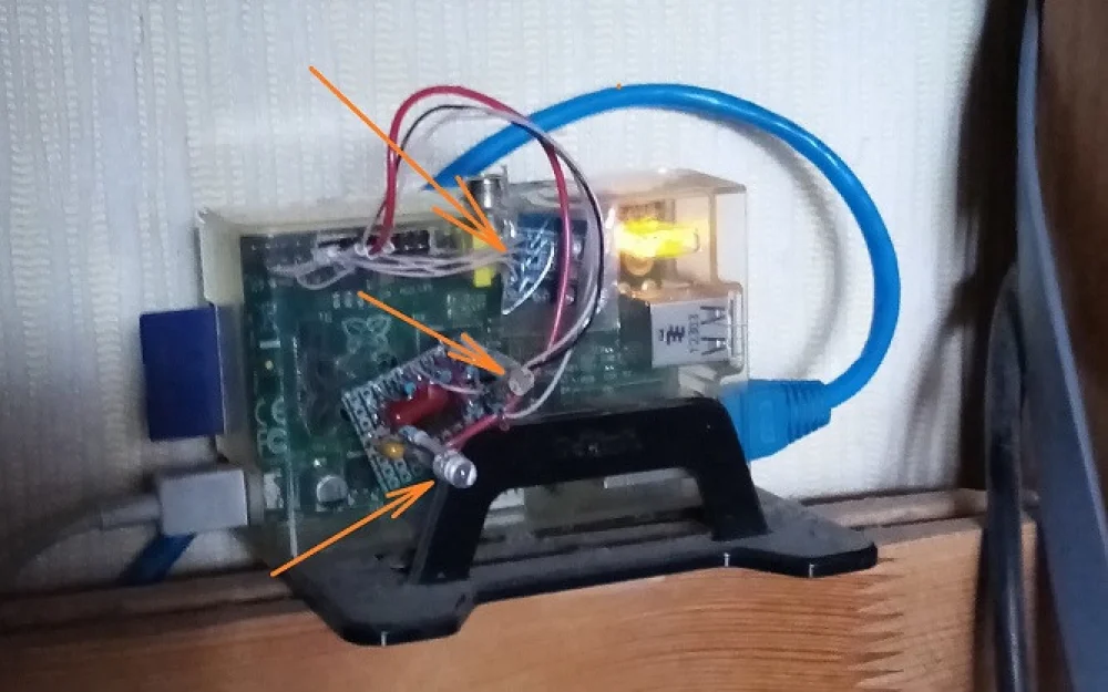
This concludes the description of the sequencer on the Antminer S9. I am now using it as part of a satellite transceiver. I will illustrate its operation with this photo.

HDL, Linux build scripts, and source code for the control program in Rust can be found here https://github.com/lesha108/sequencer.git
I hope that these articles have inspired some radio amateurs to try experimenting with Antminer S9 boards. Share your ideas in the comments, or better yet, write articles with project descriptions on Tekkix!


Write comment