- DIY
- A
About Industrial High-Speed Methods of Soldering Printed Circuit Boards and More
In the previous article, we touched on an interesting topic in the production of printed circuit boards, such as the creation of solder masks using screen printing (strictly speaking, this method is suitable not only for creating solder masks but also for applying component values on the front side of the board, as well as the mounting locations for components).
However, rapid manufacturing of printed circuit boards is also inconceivable without the use of fast soldering technologies, so let's try to figure out what such soldering technologies exist...
Here and below, we will exclusively discuss through-hole soldering technologies, without touching on SMD assembly.
I think that many who have some experience in electronic components, microcontrollers, programming, and everything around it have repeatedly thought about the fact that this knowledge can indeed be monetized!
In fact, it is about the idea that almost any area of human activity, wherever you point your finger—remains unaddressed, from the perspective of microelectronics, and automation in general.
By this, I mean not that there are no electronic components or some automation in any given area, but that in any area, a multitude of ideas can potentially be applied, which, one would think, any technician has in abundance! ;-)
Practically any electronics contain printed circuit boards, which, when manufactured, imply many quite standard stages: layout design, track fabrication, drilling (if through-hole mounting is implied), cutting boards, and several other stages, among which soldering stands out—as it significantly determines how reliable the printed circuit board will be, and how well the components will be electrically connected to each other.
Thus, if all other stages can be varied to some extent, soldering cannot be taken lightly :-)—after all, it can be fraught with consequences... Therefore, it makes sense to study (if there is any interest in this issue, and you are planning your small production (at least small, home-based))—the industrial technologies of this process, which will allow it to be carried out not only quickly but also qualitatively.
Among all modern methods of rapid soldering, the immersion soldering method can probably be named as the first.
Immersion Soldering
This method is considered the simplest and most accessible for a wide range of manufacturers/enthusiasts. In particular, this is why it is believed that this method is most widespread in developing countries, due to its accessibility—after all, essentially, all it requires is a bath with molten solder!
It is hard to disagree with the assertion about the accessibility of the technology, as a cursory review shows that the minimum versions of solder baths—priced at do not even reach 1300 rubles (at least at the moment, during the analysis of this issue):
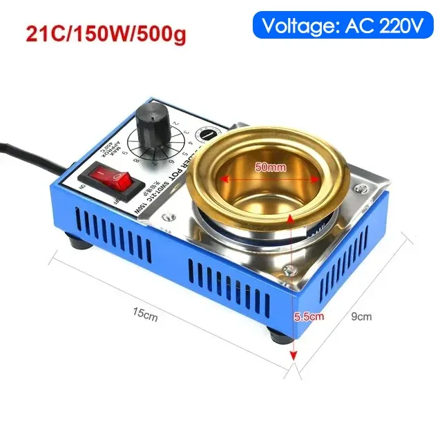
But in reality, it is only seemingly simple, as the process actually contains a series of nuances, without taking into account which nothing will work—and this will be discussed in more detail below, but first, let's take a look at what the process represents as a whole…
In general terms, it can be characterized as a method of small-scale production of products, quite inexpensive, and, as mentioned above—due to this, accessible to many.
The soldering method within the "immersion soldering" process represents (as one can easily guess from the name) a brief immersion of the printed circuit board in molten solder, the temperature of which is automatically maintained by the solder bath at a level sufficient to melt the solder.
Since the process lasts a relatively short time (about 10 seconds or less), this brief contact between the printed circuit board and the molten metal does not cause significant harm to the board material.
At the first stage, the pins of the board that will be subjected to further soldering are treated with flux — in practice, this looks like the board being dipped with its entire bottom surface into a bath of liquid flux, resulting in the entire bottom surface of the board being covered with it (including the pins for soldering).
And here’s an interesting point: depending on the type of flux (as far as I understand) — the technology may differ further!
If someone can provide more information on this topic, I would be grateful! I think I’m not the only one, as I believe readers will also find it very interesting…;-)
At the second stage, the printed circuit board is dipped into solder, where, as mentioned above, depending on the type of flux used, there are two options (please correct or add if I’m wrong):
Without preheating the board: in fact, this is one of the rather poor options for two reasons:
An aggressive, active flux is required (usually acid-based), which prepares the board for soldering in a short time by removing oxides from the soldered elements, even in suboptimal temperature conditions.
As a result, there is a need for thorough cleaning of the board after soldering, as corrosion may occur.
Also, according to several estimates, this method provides less solder joint strength than with board preheating.
With preheating the board: this means that before dipping in solder, the board, with already applied flux, is heated by any available means — for example (in the case of a more professional approach) by holding it for some time above a special infrared heater.
However, a simpler approach can also be used — holding the board a small distance (1-2 cm) above the surface of the molten solder (for about 1-1.5 minutes).
The option without heating is shown below:
The main consequence of preheating the board is the elimination of thermal shock when the cold surface of the board contacts the hot surface of the molten solder.
In practical terms, this means 2 consequences:
Solder will not solidify too quickly, which will allow it to reliably adhere to the surface of the soldered components;
an unobvious consequence* — the lack of instant solidification of the solder upon contact with the printed circuit board will allow the board to be removed from the solder without lifting half of the solder from the bath along with it! :-D
*This second point will surely not be completely clear, so it needs clarification: the thing is, when I studied all these processes for myself, I found an interesting video where a person practically demonstrates how he conducted numerous experiments, and only after that did he start achieving stable results — where one of the main problems was precisely this: the solder solidifying too quickly on the surface of the printed circuit board, resulting in a kilogram of solder or so being pulled out along with the board!
The problem was only resolved after preheating the board by holding it above the surface of the solder!
You can watch a successful experiment with detailed explanation here, starting at 8:00 (if you want to see all the unsuccessful attempts, you can watch from the beginning):
At the same time, as we can see, there is another significant point: both extracting the board from the solder and lowering it into the solder should be done at a certain angle — approximately around 45°.
Why this way: dipping the board into the solder helps to avoid the risk of trapping and holding an air bubble under the board, while when extracting, it allows excess solder to drain off more easily, as well as reduces the risk of forming parasitic bridges (solder connections in areas that were not intended).
Thus, at the final stage, it remains only to clean the board from flux residues, and that's it!
As far as I understand, the technology of simple dipping soldering is not only the simplest but also historically the very first technology for rapid industrial joining of electronic components, which emerged immediately after the transition to printed circuit boards with conductive tracks, following the departure from the stage of through-hole mounting, which occurred approximately in the 1940s…1950s of the 20th century.
Nevertheless, even from the entire description above, it is easy to guess that the technology is not the pinnacle of dreams — yes, it allows one to perform its function in a simple and cheap way, however, there is a whole mountain of caveats, among which, as we have already seen, one significant aspect can be called a certain "skill" of the hand to feel the correct angle, the right time intervals…
And besides that, despite all this, we have seen that even such experience does not fully eliminate parasitic bridges.
Well, (we have also seen this) — the constantly heated solder in the bath continuously oxidizes, which forces the operator to constantly clean it before dipping a new board — that is, aside from the actual soldering itself, one has to take care of some additional things...
By the way, while we are still on this topic, this is what a through-hole mounting looks like (for those who are not aware) — quite scary, from today’s perspective: :-)
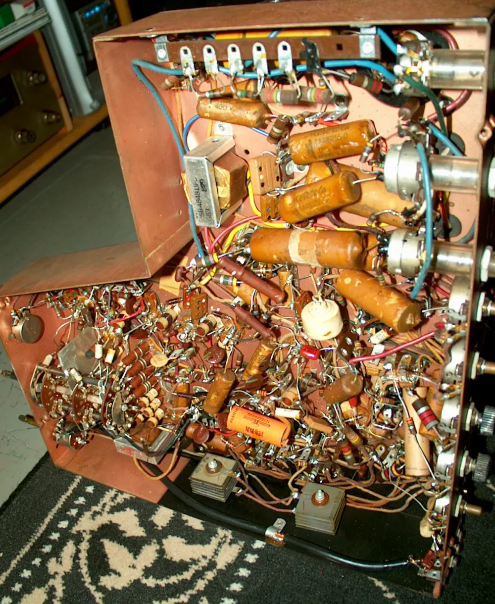
More details about through-hole mounting can be read, for example, here.
Thus, it is not surprising that engineers sought to find an alternative to wave soldering, and this alternative was found around the 1950s — wave soldering.
The main reason for switching to this technology is its pronounced ability to integrate into conveyor production lines, while the side positive aspects include reduced formation of unwanted bridges between soldering points compared to wave soldering, due to the continuous washing of the soldering area with molten solder, where the dynamic nature of this action significantly reduces the possibility of bridge formation.
But this is not the only positive aspect — during the soldering process in this way, the thermal shock to the printed circuit board is reduced, since at any given moment, the thermal impact is only on a small part of it, while the rest of the board remains unused.
As far as I can understand from the official websites of the manufacturers of equipment for conveyor soldering of this type, the process itself is very similar to dip soldering, at least it includes the same stages:
Preliminary fluxing of the board — where both acidic and non-acidic fluxes can be used for fluxing (this will depend on the further need for intensive or less intensive cleaning, for example, in an ultrasonic bath).
Fluxing can be done either using a special device where the flux is raised above the edges of an elongated bath, in the form of a "constantly boiling foam," or by spraying (as far as I understand, this is considered a more progressive option).The flux-coated board is pulled through a special heating tunnel, where heating elements (quartz lamps, in one variant) heat the lower surface of the board so that before soldering it is preheated to a sufficiently high temperature (100°C…130°C).
Then the board comes directly under the influence of a similar elongated bath, resembling a fluxing bath, except that above its edges, solder constantly flows and mixes in the form of a mound.
The temperature of the solder must be maintained within fairly narrow limits (240°C…250°C, for lead solder); otherwise, what is known as a "cold joint" may occur — a weak solder connection, cracking, insufficient wetting of the board surface with solder.
The flow of solder is ensured by a paddle wheel driven by an electric motor (in the simplest variant) or by a MHD pump (in a more modern and expensive variant).The board that has exited the soldering zone must be cooled according to a specific temperature profile, which implies a certain sequence of temperatures related to time — where, on average, the cooling rate should not exceed approximately 5°C/sec.
This cooling rate allows for the formation of a fine-grained structure of the soldered joint metal, which is the most durable.
Those who wish to learn more about modern wave soldering approaches can find a quite interesting and contemporary article here.
The process looks like this (an older version is shown, with fluxing foam):
Interestingly, at this moment, wave soldering is not even the most progressive option — and currently, selective soldering (with or without robotic drive) holds the palm of supremacy.
In the first case, the essence of the technology lies in the fact that a special container, equipped with a nozzle of a diameter most suitable for the specific case, moves along the XY axis (or only along X or only Y).
From this nozzle, at a small height, just like with wave soldering — a bubble of solder rises.
The manipulator moves this nozzle and the board, lifting it to the printed circuit board only where components need to be soldered.
Thus, the thermal impact on the board is further reduced, and during soldering, it becomes possible to combine technologies of both surface mounting and through-hole (see approximately 1:36):
Accordingly, in the second, simpler option, the board is soldered by a human operator without any manipulator:
Thus, we see that soldering technologies have progressed quite significantly over the past years, where, nevertheless, the simplest technology (dip soldering) for home use and experiments appears to be the most suitable due to its simplicity — a small bath, about the size of an A4 sheet, with adjustable temperature, what could be easier? :-)

Write comment