- DIY
- A
Power Supply Repair with Power Delivery. 470 grams of electronics
I don't like writing about tech repairs, as it's usually routine. The most common hardware issues are aging, overheating, overloads, moisture, and so on.
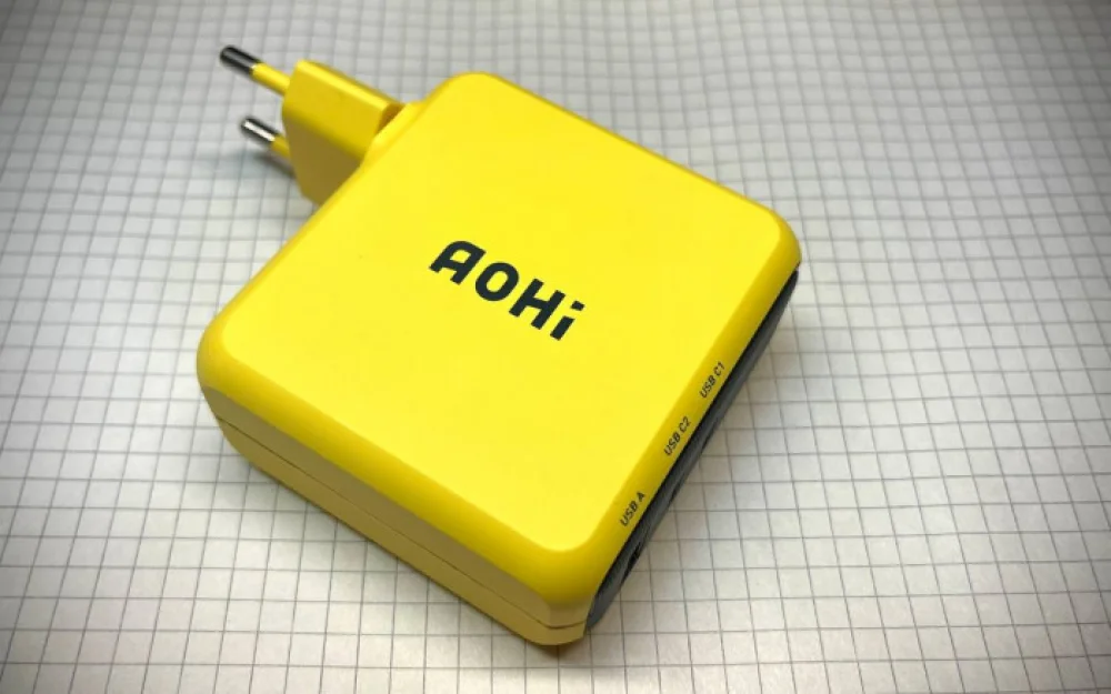
But here a colleague brought a power supply that was purchased for testing devices with Power Delivery, saying: "I charged my phone twice and the power supply stopped working." AOHi GaN 140W, weighing 470 grams (!), with relatively compact dimensions. It seems to me that for such a cost, it should have lasted a bit longer. I decided to disassemble it just to prove that there was simply a lead plate inside, and that the power supply was completely ordinary. Spoiler: no.
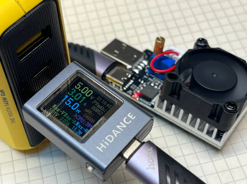
To start with, a little about its specifications. The unit has two USB TYPE-C ports and one USB TYPE-A port. The LED indicator changes color depending on the operating mode. Dimensions are 76x69x32 (without the plug). The case looks very high-quality and feels nice to the touch. There is nothing superfluous. Only the rapid failure and weight are troubling.
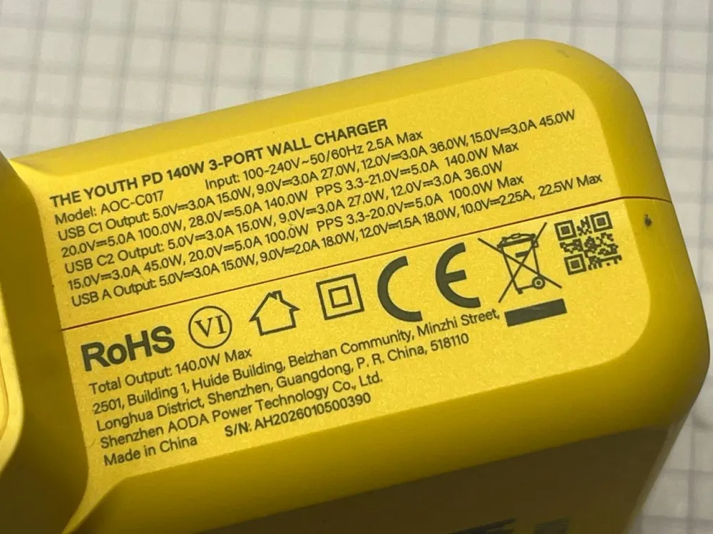
In the picture above, you can see that the maximum power of 140W is achieved at 28V. This is only implemented on the "USB C1" port, apparently to avoid total overheating if all ports are loaded. I found a list of protocols online: PD3.1 (PD3.0\PD2.0), QC4+ (QC4.0\QC3.0\QC2.0), PPS, APPLE 2.4A, AFC, FCP, SCP. This still needs to be verified in practice.
By the way, the store sent a new device set for free, and did not ask for the faulty one back. So, let's open it up.
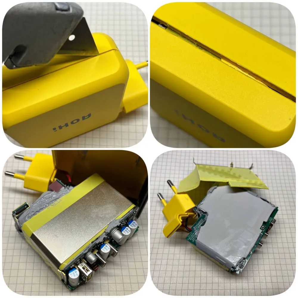
Since the halves of the power supply are held together by ultrasonic welding, the only option is to cut the case. If done carefully enough, then later you can wrap it with tape "attach" the halves with epoxy resin. The main problem with this is the closely located components inside, which can be easily damaged.
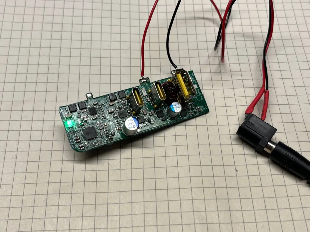
I desoldered the shields from both sides. I was pleased to find that there was no lead plate inside. The transformers and thermal conductive sealant (which is very similar in consistency to thermal pads for radiators) create a quite significant weight. It fills all the free space, except for the Power Delivery board with output connectors.
First of all, I discharged the electrolytes on the hot side to avoid excruciating pain (in the literal sense). Since there was a residual voltage of about 120V on them (I measured it beforehand), I assumed that the pulse converter was operational. This is not a panacea, but considering the total operating time ("charged the phone twice"), I move on to studying the second board.
At a minimum, it should receive power. By examining the contacts and electrolytes, I can easily find what I need and understand the polarity. I measure — short circuit. I noticed that I didn't cut the case very neatly and damaged the capacitor. I desolder it — the short circuit on the board remains, the capacitor is normal by all parameters except for its appearance.
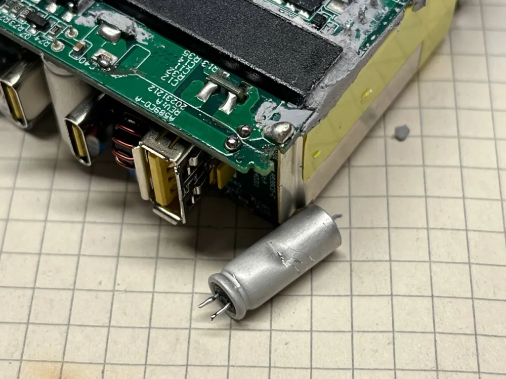
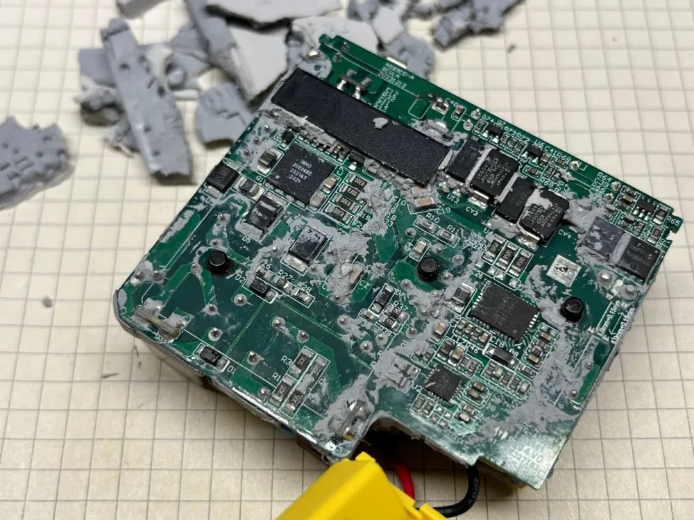
To understand where the short circuit is, I will have to desolder the PD board. What I liked is the quality of the board design. All silk-screening is preserved, while maintaining a sufficiently high density with double-sided mounting.
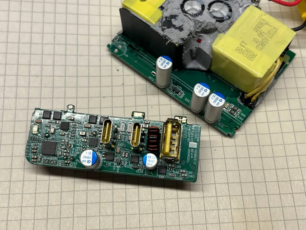
The short circuit remains only on this board. Everything is fine with the pulse unit. Let's check what the Power Delivery channels are made of — the IP6550 chip.
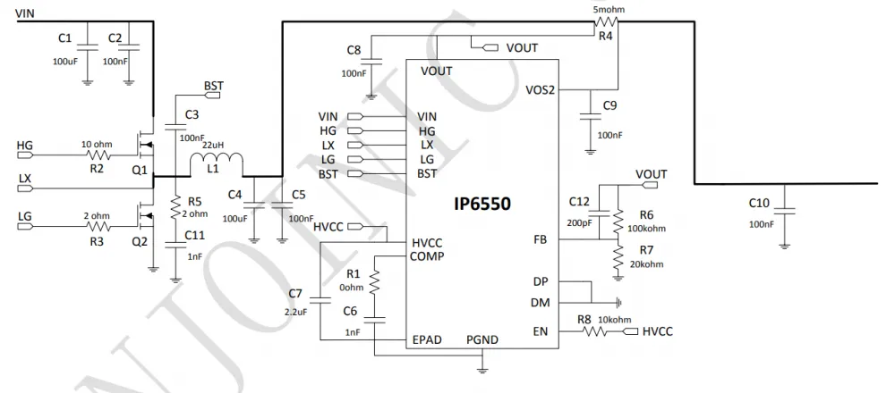
It turns out that there are several options — either the MOSFETs are blown or the chip itself is faulty on VOUT or VOS2. There can also be a short circuit in the ceramic, but that is a rare case. First, let's check the transistors. Since there are three such channels on the board, it is necessary to determine which pair has burned out. To do this, I supply 10V/1A from the external unit and observe what heats up.
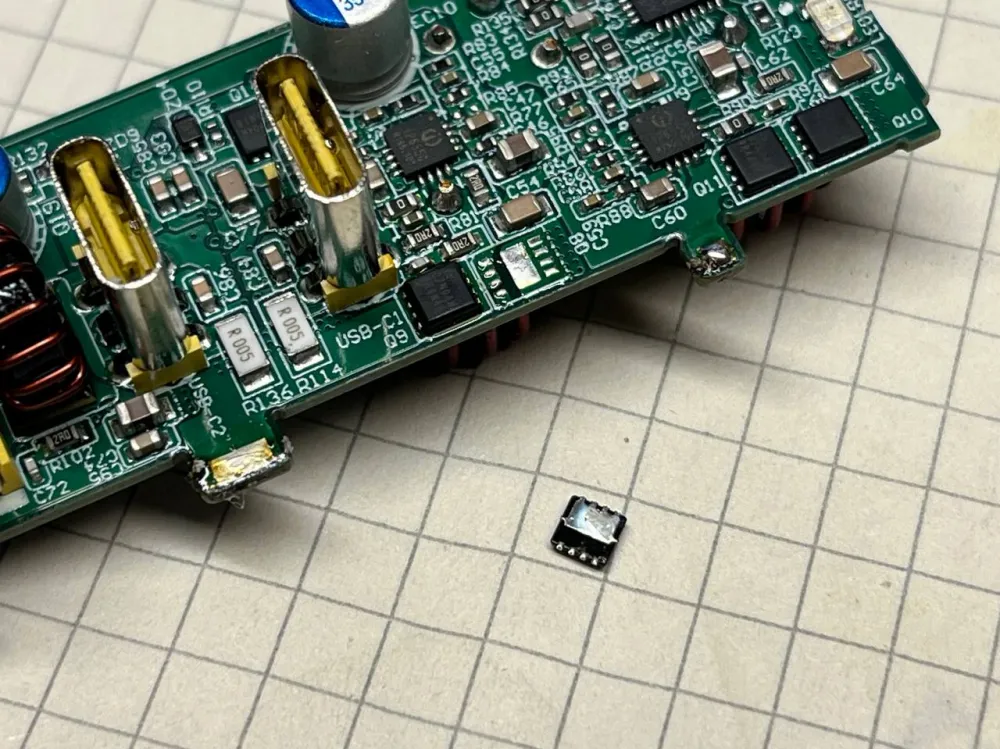
Yes, it's exactly this pair in short. After removing both transistors, the board started consuming 10mA — excellent! Powerful VSE007N04MS were installed here. I only had SiSS30DN available. To avoid losing the powerful USB TYPE-C, I took the transistors from the USB-A channel and soldered my own there. Let's check the board's functionality.
Now, what's the answer to the question of why I did all this? Well, the transistors with a current of 75A couldn't have burned out because of connecting the phone. There must be something affecting the electronics to cause all this. I put the board back in place and found that very thing!
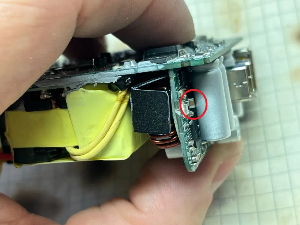
Oh dear. I discovered three such places! In three locations, when pulling the cable out of the TYPE-C connector, there is a slight deformation of the board, literally 0.5-1mm (which is already not good) and that's it. Specifically, this ceramic is positioned according to the input voltage. A couple more in other places. This is only what is visible. Perhaps there is something similar directly under the electrolytics. Once again, oh dear. To avoid having to disassemble the power supply again and change the keys (or maybe even the phone), I wrapped the capacitors with several layers of polyimide tape.
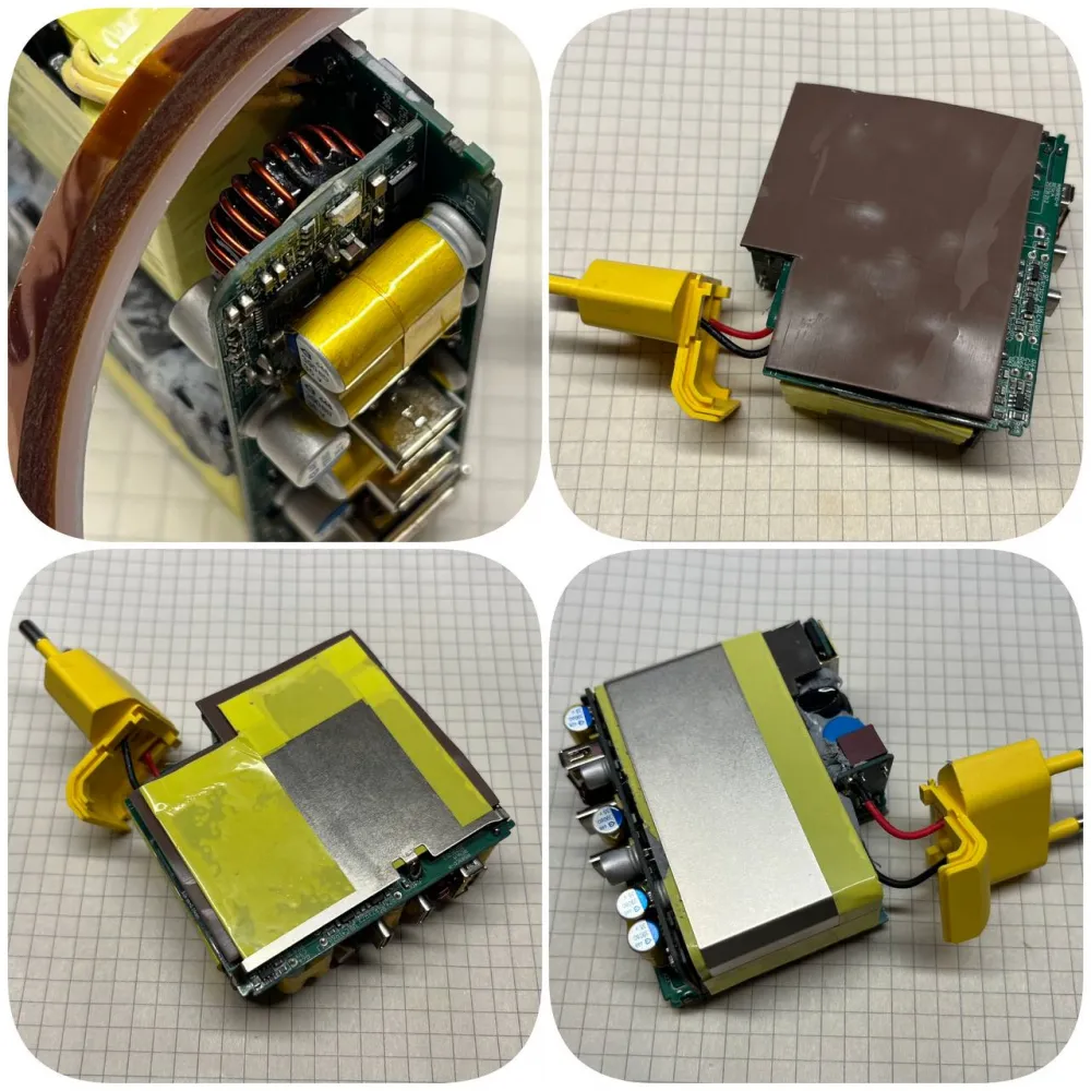
To maintain good heat dissipation, I placed two layers of thermal pads under the screens — this won't replace the original design, but it's better than nothing.
I ordered a USB-C PD load to run through all operating modes and check the heating. I don't have the desire to connect powerful devices for now; who knows if something else will come up.
At the moment, I was only able to test in 15W mode. There is, of course, no heating of the power supply. It would be good to have ten times more load.
I also acquired a USB TYPE-C trigger module so that I could set different voltages through jumpers according to the protocol. And I immediately burned out my load board. It had an unmarked LDO installed, apparently rated for an input voltage of up to 18V. I will need to try replacing it with a BD450M5FP, which can handle up to 42V. For now, I will test it the old-fashioned way – with load resistors.
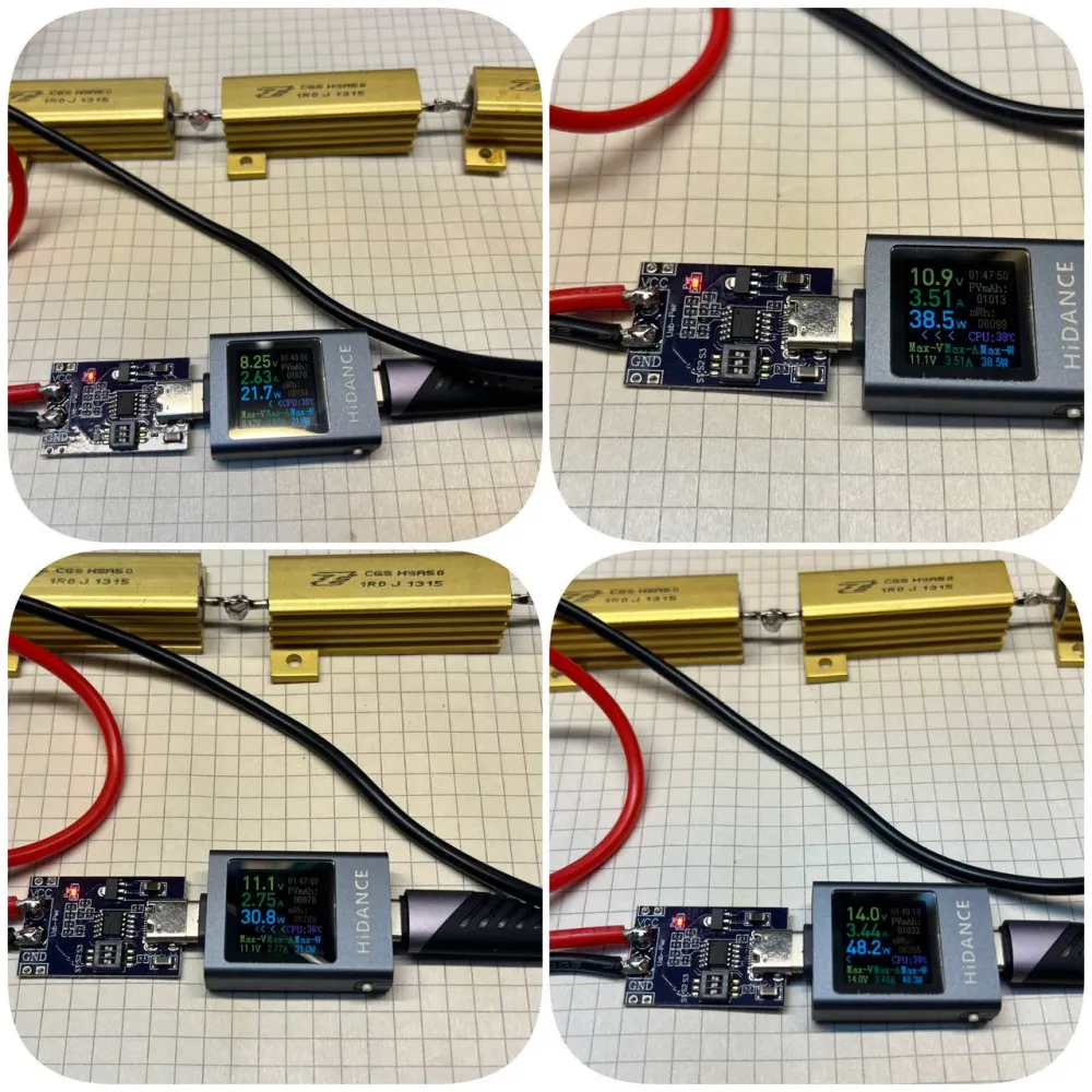
What conclusions can be drawn from this? The tests showed a voltage drop of about one volt, but at the same time, it holds current even more than stated. In principle, the power supply looks quite good quality. A design flaw renders it unusable, but I want to believe that a protective shield was forgotten during assembly, which would prevent the electrolytes from shorting the components on the board (we are currently waiting for a response from the development department, but it’s not certain that we will get one). If this is not the case, then sooner or later this problem will manifest in all such power supplies without exception.
Thank you for your attention and good luck!


Write comment