- DIY
- A
Vibe Coding for FPGAs: How I Built an I2S FIFO Retimer Without Knowing Verilog
Vibe coding seems harmless when it comes to scripts, landing pages, and small services. But what happens if you try to use it to build an FPGA project with I2S, FIFO buffer, DSD, S/PDIF, UART, PSRAM, and real hardware debugging?
Programming PLDs (FPGA) is considered the pinnacle of the digital DIY audio world.
You can implement FIFO buffers that accumulate audio data and eliminate jitter, as well as create custom digital filters with performance that far exceeds what is available in mass-produced DAC chips.
There is only one problem, but it is a significant one.
You need to learn to program in Verilog or VHDL, which are hardware description languages. Their logic differs greatly from conventional programming languages, and even from microcontroller programming.
If you do this as a hobby and you're well past your twenties, the entry barrier may seem extremely high. That's exactly why, even though I bought a Spartan 6 development kit almost ten years ago, I never got around to actually working on it.
Let's fast forward to 2026, when AI is already considered a "sort of mature" technology.
All the young people are into vibe coding these days: they simply discuss with AI what they want to build, then let the artificial intelligence write all the code for them.
After several iterations of this process, you usually end up with something that works. It may not be elegant, optimized, or secure, but at the very least, it functions. The very fact that a person with no programming skills can create a working, presumably useful program seems almost incredible.
And I thought: what if we apply this approach to FPGA design?
So I got to work, or more precisely, started exchanging messages with Gemini Pro 3.1.
Before we continue, a quick note. Not all AIs are equally capable. If you think you can pull off something like this using "free/fast" models, you're very much mistaken. You'll need all the available computing power. I managed with a basic Gemini Pro subscription for roughly $20 a month, but access to top-tier Claude models would have saved me a lot of time. For a hobby-level project, this isn't a huge problem, but it's still something to consider.
Let's get back to the main point.
After getting confirmation from Gemini that he can indeed write most of the Verilog code for me, and realizing that the Spartan 6 is already quite outdated, I started looking for a suitable FPGA.
The main requirement was that it had to be possible to actually solder it by hand. I needed to be able to solder it to a printed circuit board (PCB) without having to order a pre-assembled board manufactured. This meant no BGA packages.
I thought it over and settled on the Intel / Altera MAX 10. It has sufficiently powerful variants in a 144-pin EQFP package that can be soldered by hand. Perfect.
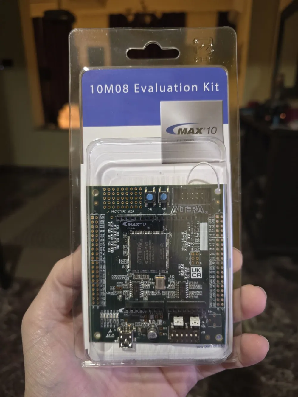
You can buy the 10M08 development board from Mouser for around 60 dollars.
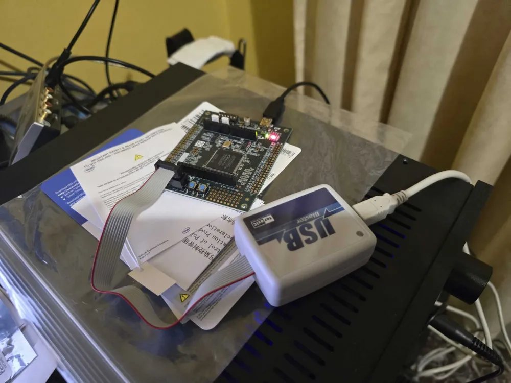
That said, the USB Blaster programmer you will also need actually costs a bit more than the development board itself. You might be tempted to buy a clone programmer on eBay. Don’t buy one of those. It won’t work, even if AI insists otherwise. I bought one, tried to get it working and failed spectacularly. I asked AI why I wasn’t having any luck, and the response was something along the lines of: “Oh, you got that cheap Chinese one? Sorry, that’s junk, it will never work, just shell out 60 dollars for a proper programmer”.
Anyway, once I had a working programmer on hand, I opened Quartus, wrote my first “blinky” in Verilog and uploaded it to the development board. The LED started blinking. Perfect.
The next step was to build something useful. With the help of Gemini, I started writing – okay, mostly copy-pasting code snippets that were supposed to implement an I2S receiver, a dual-clock domain FIFO, and an I2S transmitter, initially only for a 44.1 kHz sample rate and 32-bit depth. The plan was for PLL blocks to generate the required BCLK, LRCLK and DATA signals from the 50 MHz system clock. Part of the process came down to fighting Quartus errors, especially when trying to generate IP cores and when glitchy screens appeared in the interface. AI was a huge help here: it suggested solutions and workarounds for the errors.
Once the test project was assembled, I hooked up an Amanero as the I2S source, and a small DAC (digital-to-analog converter) based on the ES9023 as the I2S receiver. I connected the DAC's analog output to an oscilloscope and uploaded the code to the FPGA. Then I played a 10 kHz sine wave test file, and got… garbage on the oscilloscope.
Well, what did I expect? It was practically a blind stab at FPGA programming.
But then the AI magic kicked in. I explained to the AI exactly what I was doing and what I was seeing on the oscilloscope, and after a few rounds of questions and answers, it pinpointed the issue immediately. It suggested a few changes to the code, and lo and behold, I saw a clean 10 kHz signal on the oscilloscope.
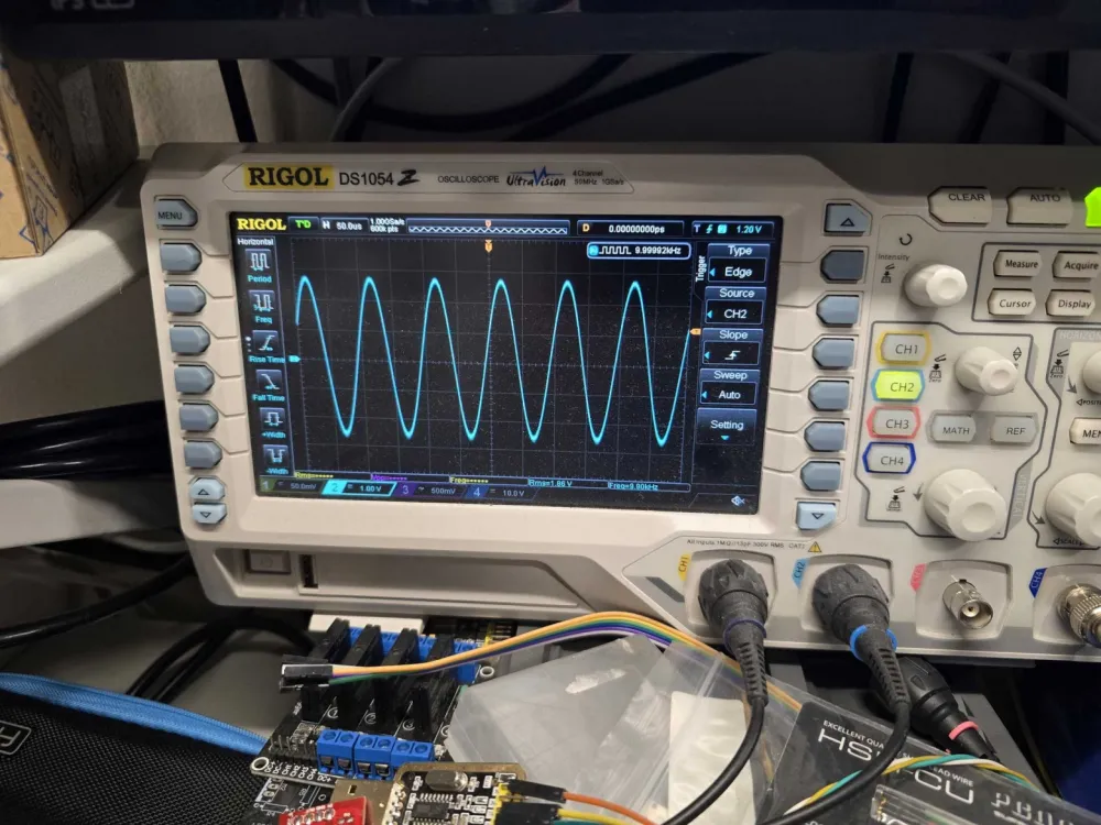
That's how I ended up with a system that receives I2S signals, buffers them in a FIFO, and outputs them via an I2S transmitter. This was the first and most important step toward what I wanted to implement, and everything was up and running after just a couple of hours of work.
And I pulled all of this off without writing a single line of Verilog code. Total victory.
The project then evolved naturally from there.
I managed to get the bit counters working to detect the sampling rate of incoming signals.
I enabled the external MCLK (master clock) so the FPGA output would run in sync with the DAC.
I enabled the bidirectional UART (Universal Asynchronous Receiver-Transmitter) to monitor what's going on inside the FPGA and send it commands: for example, switch the input, or report the sampling rate back to me.
But not everything worked right off the bat. I came up with the idea to implement a PRBS-15 test procedure to verify bit-level accuracy, to visually confirm that the FPGA wasn't corrupting my signal in any way. Gemini 3.1 Pro couldn't figure out why it wasn't working. Neither could Claude Sonnet 4.6. Or Claude Opus 4.7. So I scrapped the PRBS approach and switched to a "known pattern" recognition algorithm instead. It worked immediately, and that was more than sufficient.
Next, I added DSD compatibility with automatic signal type detection.
And a DoP decoder.
And protection for DSD against stuck bits.
And a full bit depth detector.
And LEDs that indicate the status of the FIFO buffer, as well as the bit depth and DSD attenuation.
And multiple I2S inputs.
And an S/PDIF receiver with decoder, implemented inside the FPGA.
Artificial intelligence was also extremely helpful in creating the SDC file (Synopsys Design Constraints, a project constraint file) for the project. This file is mandatory when working with high-frequency signals that are sensitive to jitter.
During our discussions, I often had to remind the AI what we had already implemented, due to the limited size of its context window. But overall it performed very well.
There were also instances where it hallucinated, which led me down the wrong path and wasted my time.
But the real test of the AI's capabilities, as well as my patience, began when I moved on to adding a PSRAM chip (pseudo-static RAM) to extend the buffering time.
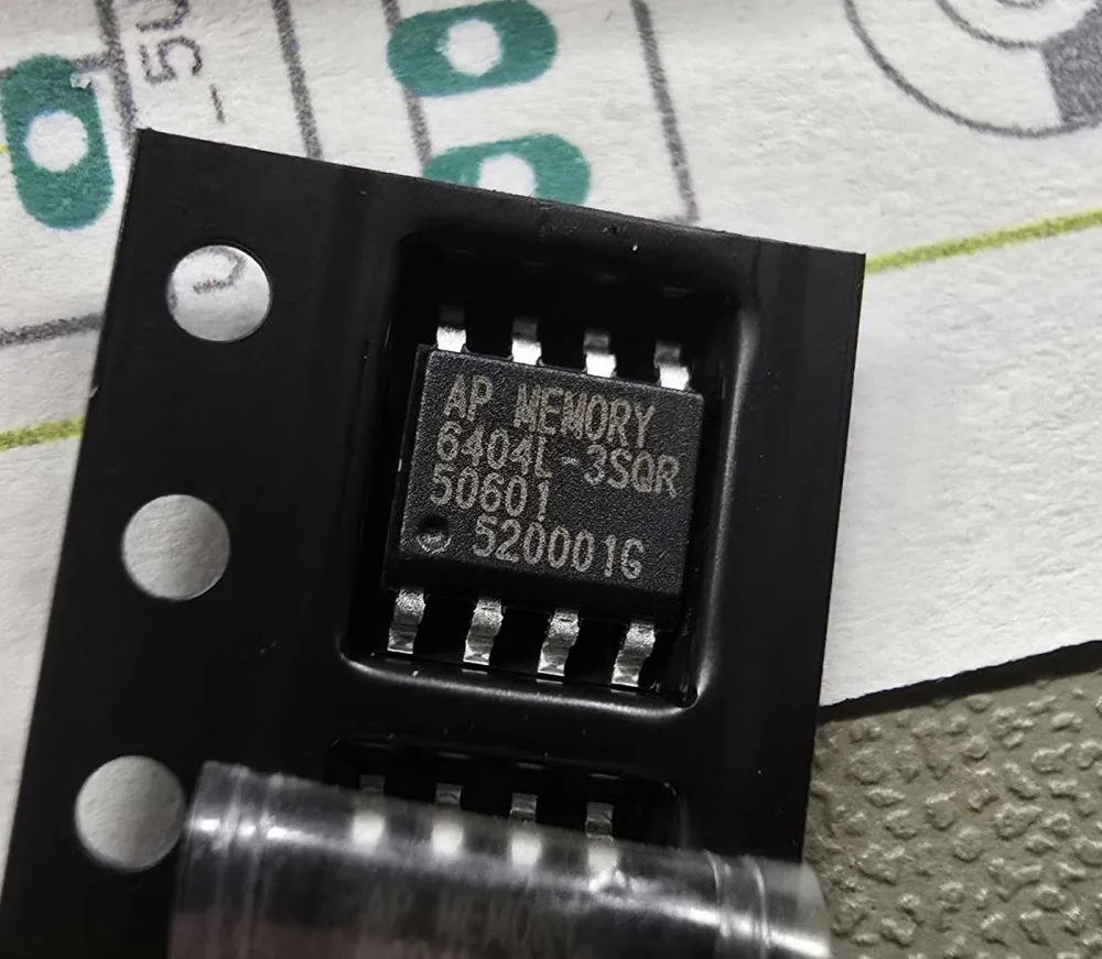
This turned out to be a serious challenge. The AI wrote a set of procedures that managed communication with the PSRAM over the QSPI bus, data processing and packing, pseudo-parallel read and write operations to memory, and a whole host of other tasks.
Of course, it didn't work on the first try.
Nor did it work the second time.
Nor the third.
Around this point I realized that staring at the blurry image on the oscilloscope screen, describing to the AI what I saw, and waiting for it to figure out on its own where exactly the problem lay was no longer enough.
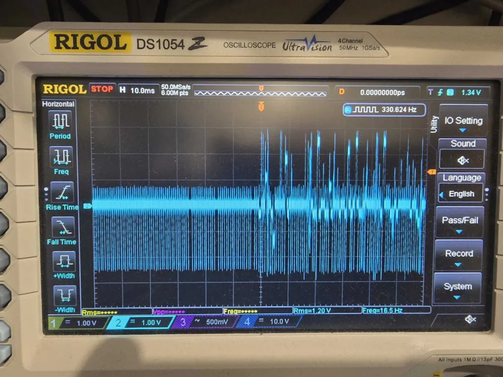
So I asked the AI to break the FPGA architecture down into smaller, individually testable parts. It agreed this was a good idea and proceeded to do exactly that. We wrote procedures to check PSRAM data for corruption, used LEDs for diagnostics, and UART to retrieve large volumes of debug information. But even with all this, we still couldn't make progress beyond a certain point.
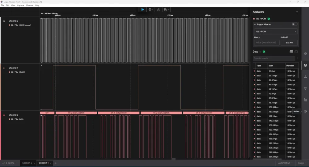
In the end, I had to pull out my Saleae logic analyzer and do classic debugging: feed it known signals and observe what the code does with them. It worked. Soon after, my FPGA was already successfully using a 64 Mbit PSRAM as a buffer and operating with bit-level precision.
That’s what I’ve been working on for the past twenty days.
It was really interesting to get hands-on insight into exactly what FPGAs are capable of. For example, a real eye-opener was realizing that the functional blocks I build essentially run in parallel, and there’s no such thing as shared "processor time" divided between components here. That’s the deterministic nature of these devices. A signal with specified characteristics will always be processed at the same speed, no matter how complex the rest of the project becomes. I can just add modules that "tap into" the same signal and do something with it, with no impact on the original signal processing.
I have to say, it’s been a long time since I found digging into a "new technology" this engaging. It was extremely satisfying to realize that a project of this complexity could actually be vibe-coded. Although in the end, I did pick up a little Verilog. Not because I had to, but because I wanted to.
So, can any person simply pick up a development board and end up with a working FIFO reclocking circuit?
That depends on how well you understand DAC architecture.
You will have to explain to the AI exactly what you want to achieve, and guide it toward the goal step by step. But you can’t just tell it: "Build me an FPGA that performs FIFO buffering for I2S and DSD signals" and expect it to pull it off. If you give it a single prompt describing the entire plan, even an extremely detailed one, it will almost certainly not work, and you’ll then have to painstakingly figure out exactly what broke.
So the process will take time.
But if you’re persistent and have a logic analyzer on hand, you’ll eventually get there, just like I did.
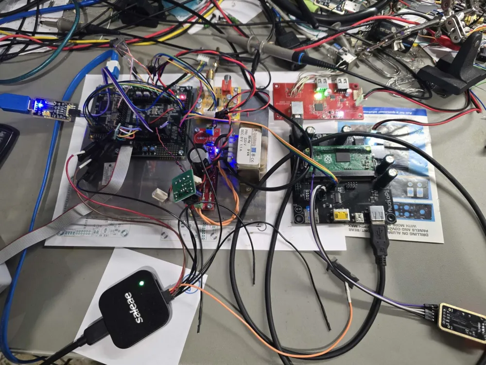
The next step will be developing a custom PCB for the FPGA and the required reclocking stage that comes after it.
Write comment