- Hardware
- A
Inside the ALU of the 8085 microprocessor
The arithmetic logic unit is a fundamental part of any computer that performs addition, subtraction, and logical operations, but its operating principle remains a mystery for many. I have reverse-engineered the ALU scheme of the 8085 microprocessor and in this article, I explain how it is structured.
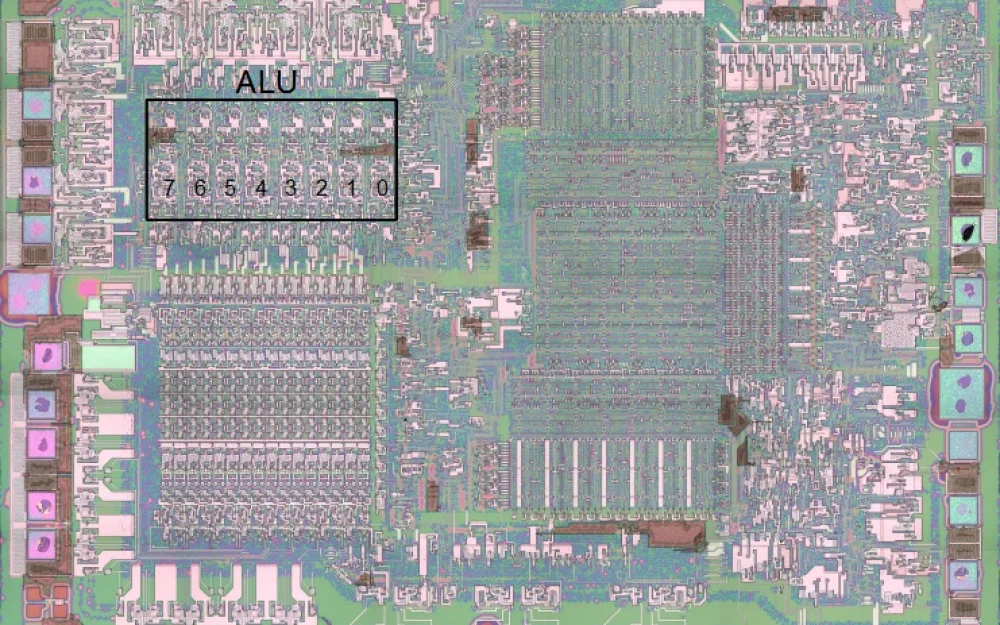
The next diagram shows the location of the ALU inside the 8085. The ALU is 8-bit wide, with the most significant bit on the left. The register file is a large block below the ALU. The registers are 16-bit wide and consist of pairs of 8-bit registers. Interestingly, in the register file, the most significant bit is on the right, meaning the order is opposite to that in the ALU.
The ALU takes two 8-bit inputs, which I will denote as A and X, and performs one of five basic operations: ADD, OR, XOR, AND, and SHIFT-RIGHT. Additionally, if input X is inverted, the ALU can perform subtraction and complement operations. You may notice that SHIFT-LEFT is missing from this list. However, it is implemented simply: the number is added to itself, which is equivalent to a left shift by one bit in binary representation. Note that the arithmetic operations in the 8085 are very basic. Multiplication and division are absent—they only appeared in the 8086.
The ALU consists of 8 nearly identical blocks, one for each bit. During addition, each such block adds the corresponding input bits, computing the sum A + X + the input carry, forming the sum bit and the output carry bit. That is, each bit of the ALU implements an
ALU Diagram
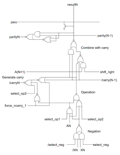
The diagram below shows one bit of the ALU. Overall, the diagram mirrors the physical implementation on the chip, unfolding from bottom to top. Eight such blocks are arranged side by side, with the least significant bit on the right. Carries propagate from right to left, and bits during right shifts—from left to right.
Inversion
At the bottom of the diagram is a complex logic element labeled Negation ('Inversion'). This element, when necessary, selects the inverted second argument, providing either XN or /XN. (XN is the Nth bit of the second argument, which I denote as X. The symbol / means complement.) To simplify further explanation, let's assume that XN is not inverted.
Operation
Above the complement selection block are several logic elements labeled Operation ('Operation'), which perform the required two-input operation. The NAND element on the left forms either A NAND X or 1, depending on the control line select_op1. The OR element on the right forms either A OR X or 1, depending on the control line select_op2. Combining these signals through NAND yields four possible results:
select_op1 | select_op2 | Result |
0 | 0 | A NOR X |
0 | 1 | 0 |
1 | 0 | A NXOR X |
1 | 1 | A AND X |
Note that instead of OR and XOR operations, their inverted value is obtained at this stage. This will be corrected in the next step.
Combining with Carry
Above the operation block is the next node, labeled Combine with carry ('Combining with Carry'). It forms the ALU output by combining the input carry with the operation result using XOR.
To understand the operation of this node, first consider the simple XOR element, which is used multiple times in the ALU. Its logic is quite simple: if both inputs are 0 (upper case) or both are 1 (lower case), then the output is 0.
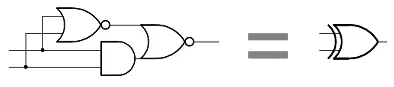
If we temporarily ignore the right shift circuit, this logic block effectively represents an XOR. Here, XOR with 0 changes nothing, while XOR with 1 inverts the value. The expression A XOR X XOR CARRY corresponds to the least significant bit of the sum of A, X, and CARRY.
The key idea of this unit is that the input carry is formed to convert the operation result into the final correct value. The input carry /carry(N-1) can take the value 0, 1, or the inverted carry from the previous digit—depending on the operation.
Op | Operation Result | Carry | Result |
or | A NOR X | 1 | A OR X |
add | A NXOR X | /carry | A XOR X XOR CARRY |
xor | A NXOR X | 1 | A XOR X |
and | A AND X | 0 | A AND X |
shift right | 0 | 0 | A(N+1) |
complement | A NOR /X | 1 | A OR /X |
subtract | A NXOR /X | /carry | A XOR /X XOR CARRY |
Note that the input carry line must take the correct value to obtain the desired result. In addition, it transmits the inverted carry from one digit to the next. For OR and XOR operations, it is set to 1. For AND and SHIFT_RIGHT, it is set to 0. As will be shown below, the carry generation circuit provides the required value for each operation.
The last element of this circuit is the right shift block. When the operational input is zero, the carry is zero, and the shift_right signal is active, the output receives the bit from the adjacent right digit: A(N+1).
Carry Generation
On the left is the Generate carry node («Carry Generation»), which computes the output carry. It can output three possibilities: 1, 0, or (inverted) carry from the sum. If the select_op2 line is active, the carry is forced to 0. If the force_ncarry_1 line is active, the carry is set to 1. Otherwise, the carry is computed for the sum A + X + input carry according to standard logic: if the input carry is 1 and at least one of the input bits is 1, a carry is generated. If both input bits are 1, a carry is also generated.
Flags
In the 8085, there is a parity flag that is 1 if the number of set bits is even, and 0 if it is odd. The parity flag is formed by applying XOR to all result bits (with subsequent inversion). Each bit is sequentially combined via XOR with the accumulated parity value of the lower-order bits using the parity circuit located at the top of the diagram. The same XOR element described earlier is used.
The zero flag is computed using a simple circuit: each result bit controls a transistor that pulls the zero line low if that bit is 1. As a result, an NOR gate with eight inputs is formed, distributed throughout the ALU.
Control Lines
As can be seen in the diagram, the 8085 uses several control lines to manage the ALU operation. In total, the ALU supports 7 different operations, and the table below lists the control signals used for each of them. The opcodes that invoke the corresponding ALU function are also provided.
Operation | select_neg | select_op1 | select_op2 | shift_right | force_ncarry_1 | Opcode |
|---|---|---|---|---|---|---|
or | 0 | 0 | 0 | 0 | 1 | ORA,ORI (and by default) |
add | 0 | 1 | 0 | 0 | 0 | INR,DCR,RLC,DAD,RAL,DAA,ADD,ADC,ADI,ACI (and undocumented LDSI, LDHI, RDEL) |
xor | 0 | 1 | 0 | 0 | 1 | XRA,XRI |
and | 0 | 1 | 1 | 0 | 1 | ANA,ANI |
shift right | 0 | 0 | 1 | 1 | 1 | RRC,RAR (ARHL) |
complement | 1 | 0 | 0 | 0 | 1 | CMA |
subtract | 1 | 1 | 0 | 0 | 0 | SUB,SBB,SUI,SBI,CMP,CPI (DSUB) |
The ALU control lines are generated from the opcode using a programmable logic array (PLA). In particular, these are the outputs of the PLA F block, located to the right of the ALU. This is described in more detail in my article about the PLA.



![From Virtual Hands to AI for Survivalists: Curious Open Agent OSes [and One Hardware Project]](https://cdn.tekkix.com/imgs/2026/05/habrcom/big/ce0b1057616faed51cd8b9f3b2b9.webp)

Write comment