- Hardware
- A
New DRAM is 1000 times faster than conventional DRAM, and it can transform the computing world
While we are growing accustomed to the fact that RAM prices have surged more than 200% over the past year and show no signs of dropping in the foreseeable future, the University of Tokyo has quietly unveiled a device that could upend this entire trend.
The new device switches bits in 40 picoseconds — 1000 times faster than modern DRAM can manage. And it does so with almost no heat generation. This technology could change not only the memory market, but also the entire computer assembly architecture we have all grown accustomed to. It is definitely worth taking a closer look at this to understand exactly what we will get in the future, and how our computers will operate.
New Type of DRAM
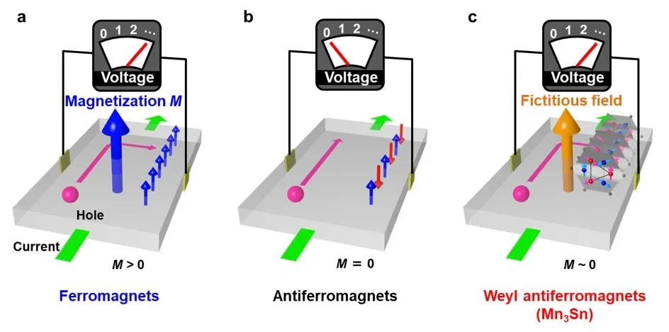
If we set aside unnecessary details that do not change the overall picture and contribute little to understanding the issue, we can say that researchers built a microscopic device from layers of two materials. These are the antiferromagnet Mn₃Sn (manganese-tin) and tantalum. They are constructed on a standard silicon substrate, as it is perfectly suited for this task.
Researchers have learned to switch the magnetic state of this device using ultra-short electrical pulses. Everything works as standard here: one state is "0", the other is "1". Between pulses, the cell stores a bit even without power, just like Flash in SSDs.
The three most interesting parameters here are as follows. Switching takes 40 picoseconds. For comparison, DRAM operates on the nanosecond scale, meaning it is roughly 1000 times slower. The temperature rise of the cell itself during switching is approximately 8 degrees. This is critically important, because most previous experimental "ultra-fast" memory technologies heated up to hundreds of degrees at the same speed, rendering them useless. Additionally, this memory is non-volatile, and bits are stored in it without power, unlike DRAM which requires constant refreshing.
What the New Memory is Used For
Every type of memory in a modern computer has its own unpleasant trade-off. DRAM stores bits as charge in tiny capacitors, which constantly "leak" — so the system rewrites them thousands of times per second, consumes energy, and generates heat even when idle, and loses all data when power is cut off. SRAM in the processor cache is very fast and does not require constant refreshing, but it uses six transistors per cell compared to one for DRAM, which is expensive and impractical. Flash in SSDs stores data without power, but switches slowly, and cells wear out quickly.
For nearly 30 years, the industry has been searching for universal memory. Something hypothetical that could combine DRAM density, SRAM speed, Flash non-volatility, and low power consumption. This may seem like a utopia, but some developments, such as MRAM, PCM, FeRAM, and ReRAM have indeed existed. However, most of them ended up being used only in niche applications. Spintronic memory based on Mn₃Sn is another attempt to reach that same goal.
What is spintronics and what does manganese have to do with it
The idea behind spintronic memory is simple: store a bit not as charge, but as the magnetic state of the material. There is nothing new about the method itself, as hard drives have been using magnetic recording for decades. The only problem is that HDDs are huge spinning platters, and we need something microscopic, solid-state, and fast.
As an experiment, researchers tried ferromagnets such as iron, cobalt, and nickel at different times, but adjacent cells interfered with each other due to their own magnetic fields. The new antiferromagnet is structured differently. Adjacent magnetic moments point in opposite directions and cancel each other out.
Externally, the material is almost non-magnetic, does not interfere with neighboring cells, and can be remagnetized several times faster. The key mechanism that allows all this to work with almost no heating is called angular momentum transfer in Russian. A current pulse remagnetizes the material not through heating, but directly — by twisting the magnetic moments into the required position. This is what made the temperature rise negligible compared to other developments.
Laser memory and what it will change
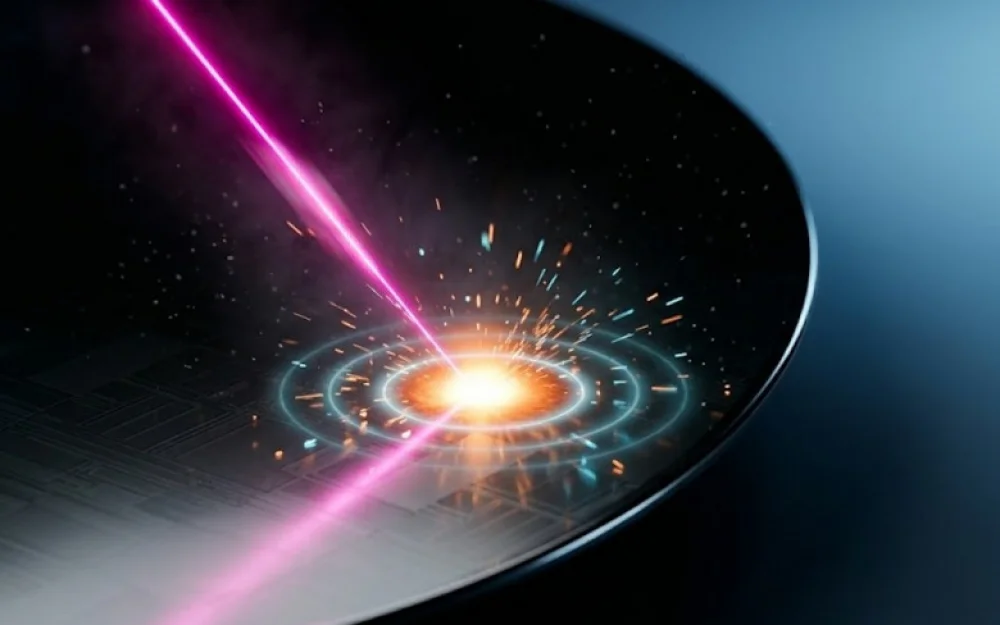
It is also interesting that the cell was able to be switched using a photocurrent pulse from a regular telecom laser. This is the band used in fiber-optic internet networks. The laser strikes a photodiode, which outputs a 60-picosecond electrical pulse that switches the magnetic state. Thus, the researchers have effectively demonstrated the possibility of writing directly with light, without a separate step involving an electronic signal.
In modern data centers, the main bottleneck is data transfer between chips, not the computations themselves. All of the world's largest cloud operators are investing in silicon photonics and optical interconnects. Memory that can be written to directly with a laser fits perfectly into this picture. For now this is only a laboratory experiment, but the chosen direction is very promising.
Modern AI accelerators spend more energy on moving and updating data than on the actual computations themselves. As GPU clusters scale up to hundreds of thousands of accelerators, power delivery and cooling become the key bottlenecks. Solving this problem would make it possible to save a huge amount of money currently spent on cooling.
Indirectly, we can note the record shortage of DRAM itself. Memory for AI servers consumes the production capacity of almost all factories worldwide. Against this backdrop, any DRAM competitor that barely even heats up is an absolute dream for the industry. But this advantage is somewhat overblown. It is unlikely the technology will be rolled out quickly enough, meaning the crisis will have ended before it even hits the market.
Read also: What will become more expensive after RAM in 2026
When will the new memory be released
And this is where the reality check begins. What was shown in Tokyo is only a laboratory structure the size of a speck of dust, not a chip ready for mass production. There are usually ten to fifteen years of engineering work, refinement and testing between such a prototype and a box on a store shelf. And that's only if the project doesn't get shut down due to emerging issues, which are literally right on the surface.
The main problem is that reliable switching requires an external bias magnetic field. That's acceptable for a lab or, at a stretch, a data center, but for a commercial chip it's a dealbreaker. No one will install a separate magnet next to the memory in a laptop. This issue, just like the scaling issue, still has yet to be resolved.
Here's the bottom line. The memory shown in Tokyo is not new memory for gamers, and headlines in the vein of "DRAM is obsolete" can be safely skipped. This is a step in the long engineering race for universal memory that the industry has been pursuing for thirty years. But it's an important step, because for the first time it was possible to combine picosecond-level speed and almost no heat generation in a single cell, with the ability to write via laser.
If the technology is brought to mass production, it will change not only memory, but the very approach to how computers store and transfer data. For now, we're still paying for DDR5 as if it were a team of three horses, putting up with smaller SSD capacities and waiting for any "future standard" to finally make it to mass production. Let's hope this isn't just another dead end, but at least some hope.
![From Virtual Hands to AI for Survivalists: Curious Open Agent OSes [and One Hardware Project]](https://cdn.tekkix.com/imgs/2026/05/habrcom/big/ce0b1057616faed51cd8b9f3b2b9.webp)
Write comment