- DIY
- A
DIY: Creating New Components in LibrePCB
When designing boards in any software, you sometimes need components that are not included in the standard package, such as a connector of unusual size or a pre-made module.
I'm currently using LibrePCB, and I saw a question in the comments: where do you get components for LibrePCB if they aren't found there?
Well, create them, of course!
Creating a new component may seem complicated at first, but in reality, it's quite simple if you understand the logic behind how it's done there.
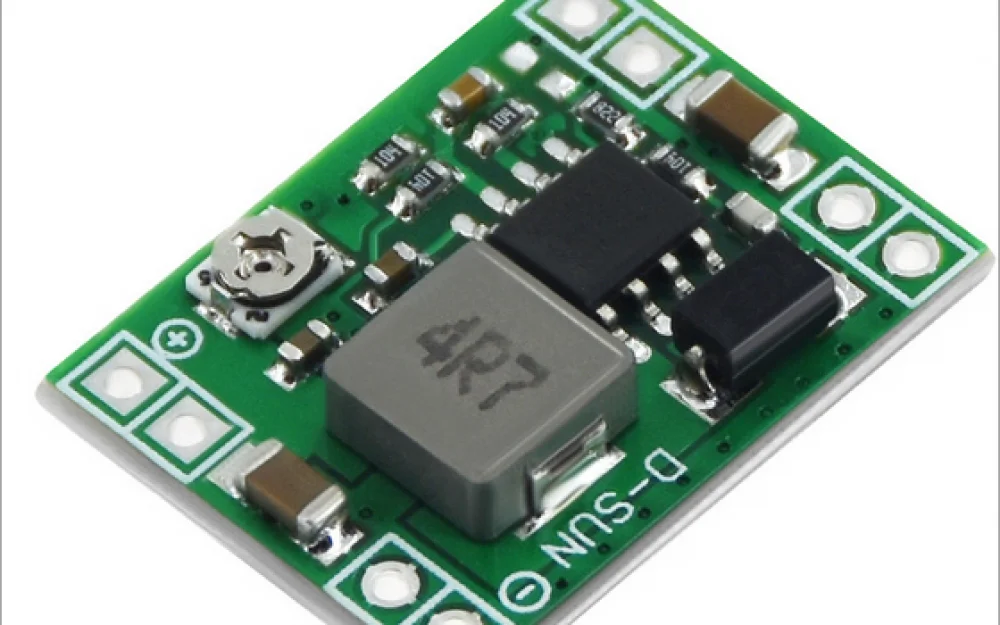
For example, let's create a DCDC voltage step-down module component:
It can be placed on the board almost like any other integrated circuit, but for that, there must be a corresponding component in the component library.
Open the Library Manager, create a new local library, and start editing it:
You'll be greeted by 6 sections: Component categories, Symbols, Component, Package Categories, Packages, Devices.
And you can create something in each of them (Ctrl-N).
In fact, it's simple: the first three are responsible for the image in the schematic, the next three for the image on the board.
Each group is "device category, type, and specifics."
Component categories, unsurprisingly - component categories: the program already has basic categories like "transistors," "resistors," and so on, but you can create your own.
For example, this particular module clearly doesn't fit into discrete components, integrated circuits, or development boards.
So, you can create a category specifically for such modules, called Modules. When creating it, there will be a field called Root category - it helps build a category hierarchy, but in this case, you can leave it empty, and it will create the root category "Modules".
After saving changes, library re-indexing occurs, which takes some time, and you need to wait for it to finish before making any further changes.
Symbols - these are responsible for the images of the elements in the schematic. If it were a known component, like a transistor, there wouldn't be a need to create a new image, but since we have a new module.
There’s also a Category field - which category it will belong to: besides the built-in ones, now there will also be our new category "Modules".
Using the built-in editor, a schematic representation is drawn cell by cell: a rectangle, several input-output contacts, labels for them.
If something is done incorrectly, the system will remind you, offering to fix it or ignore it.
Component - this is like specifying exactly which component is being created.
For example, we created an image for a step-down DCDC module, but we have several variants of such a module. On the schematic, they will look the same, be in the same category, but these will be several different components with different names.
The next block is footprint, the component’s projection onto the printed circuit board.
Similarly to schematics - Package Categories - the category of elements.
We look again at what exists, don’t find a suitable one - we create Modules (but this is a category for boards, not for schematics!).
Packages - the most important stage, here we define the layout on the board: pins, schematic representation of dimensions.
Drawing is no more difficult than in a grid notebook. The cell size is adjustable, including the possibility to change units: mil or mm.
The thing is, almost all electronics is measured in mil, which is an imperial system.
For example, the pitch of a standard pin header is 100 mil, approximately 2.6 mm.
The pitch of IC pins, relay contacts, and many other things is also in some multiple of mil: 50, 100, 200, 300...
However, since China uses the metric system, and the module’s board is Chinese, it is sometimes more convenient to switch the grid to mm, so you don’t have to deal with 787.4 mil, but just take 200 mm.
The process is not complicated: look at the module board, measure the distances between the contact holes, convert them to mil - and place the pads on the grid.
To convert, it is enough to multiply millimeters by 39.37 and then round to the nearest "nice" number: for example, 2.6 mm becomes 102.36, but such sizes don’t exist, the actual is 100, and the error is clearly a result of measurement inaccuracy.
Conversely, if the conversion to mil gives a result like 787.40 - the nearest "nice" numbers would be 750 and 800, neither of which when converted back to mm matches reality, so it is most likely metric 20 mm.
To simplify calculations, I made myself a little script: entered mm - got in mil:
#!/usr/bin/perl

print "Enter mm and press ENTER:\n> ";

while(my $str = <>){
  if($str =~ /([\d\.]+)/){
    my $mil = $1 * 39.37;
    printf("%.02f -> %.02f\n", $1, $mil);
    print "> ";
  }
}
After the printed projection is drawn, we create the device in Devices: conditionally, the same size can have different devices, just as different transistors, chips, and so on can be in a TO-92 package.
When creating the device, its category is specified, which Symbol is used on the schematic, and how it looks on the board.
That’s it, now the module can be added to the schematic, and it will appear when placing it on the board.
The same principle applies to creating a "relay": we search for or create categories like "Electromechanic devices", draw a schematic image of the "relay of this type", then create the component "this specific relay", then show it "on the board", and finally create the device corresponding to a specific schematic and a specific projection on the board.
Moreover, the distances between the pins of the relay will definitely be multiples of mil – just measure them with a regular ruler in mm, convert them to mil, and round them.
In general, nothing complicated.

Write comment