- Gadgets
- A
Part 6: PCB Manufacturing – Experience with JLCPCB
Previous part
Part 5: Algorithms – Implementation and Error Model
Preface. Today I will tell you little about the technique, but a lot about the practical part of working with component suppliers, using the well-known service JLCPCB as an example. I will talk about the difficulties we encountered and how we managed to solve them. So, if you prefer a technical storyline, feel free to skip the article.
Article Plan: This part covers the practical process of manufacturing the printed circuit board for our device:
Preparing documents for production: generating Gerber files, bill of materials (BOM), and placement files (CPL).
Selecting components in the JLCPCB library: how to choose available components or replace unavailable ones, using the Global Parts option.
Placing the PCB and assembly order: a step-by-step guide to filling out the order parameters on the JLCPCB service, features of a combined PCB and assembly order.
Cost and timing: analyzing the final price, the cost structure (PCB, components, assembly work, delivery) and manufacturing times.
Results: received boards, assembly quality, further steps for checking.
Preparing for Production: Gerber, BOM, CPL
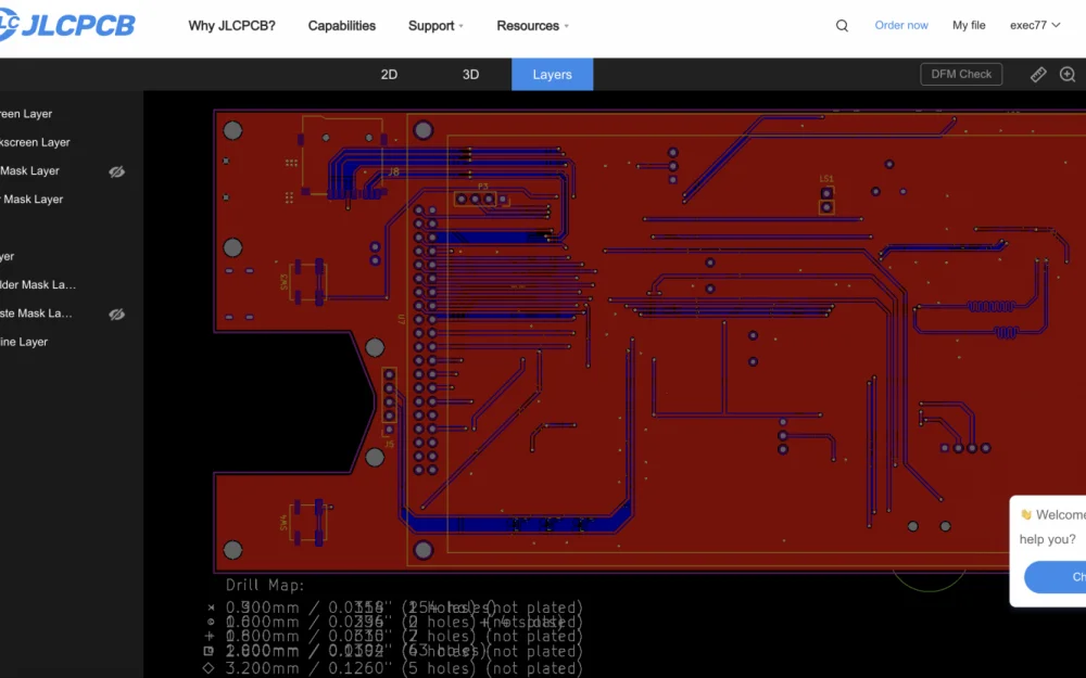
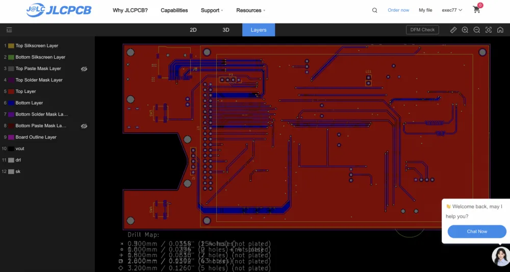
After developing the schematic and PCB layout (in CAD, such as KiCad), the next step is preparing the files for production. Typically, we needed:
Gerber files – a set of files describing the layers of the board (copper layout, mask, silkscreen, etc.) plus a drilling file. These are usually obtained by exporting from the PCB system (in KiCad, there is
Plotfor Gerber andDrill Filesfor drilling). All Gerber files are packed into a zip archive.BOM (Bill of Materials) – the list of components. It includes positions, names or designations of components (matching the schematic), their type, value, package, and most importantly – the identifier from the manufacturer's libraries (MPN or LCSC code for JLCPCB). BOM can be exported from the CAD system or manually filled out in the Excel template from JLCPCB.
CPL (Pick-and-Place file) – a file with the component placement coordinates. This file contains the RefDes (e.g., U1, R5…), X, Y coordinates on the board, layer (Top/Bottom), and rotation angle for automated assembly. The file format is CSV or XYRS and is also exported from the PCB system.
We carefully checked that the positions in the BOM and CPL match (the same RefDes) and that all required parts are present. It is especially important that the BOM includes correct LCSC part numbers – the part identifiers from JLCPCB's catalog. This will determine whether the factory can source the necessary components.
After uploading the Gerber file, BOM, and CPL, a check will be performed, and the system will create a virtual prototype of the board for DFM analysis.
Component Selection: JLCPCB Library and Replacements
When designing the device, we tried to use components that are available for assembly at JLCPCB. JLCPCB has its own library (catalog LCSC) from which they can directly install parts. Each component has a unique code (e.g., Cxxxxx). Ideally, it's enough to select the needed items from the catalog and specify them in the BOM.
However, not all the required chips were available. For example, our main microcontroller, STM32F407IGT6, was not listed among JLCPCB's core stock items. The same applied to some of the inertial system sensors. In such cases, there are several options:
Search for alternatives: Sometimes it is possible to replace a component with a similar one available in the library. For example, another MPU or accelerometer, if it is compatible in terms of characteristics and pinout.
Global Parts / Extended Library: JLCPCB offers an extended component selection. You can specify almost any MPN, and they will try to source it specifically (the so-called Global Sourcing). In our case, we used this for the STM32 and a key sensor—adding their MPN to the BOM with a "Global" tag.
Your own components (Consigned): There is an option to send your own parts, but it is more time-consuming and complicated (they need to be physically shipped). We did not use this, preferring global ordering.
To simplify the selection, JLCPCB has a convenient BOM analyzer interface. We uploaded our BOM file, and the system automatically matched items with their catalog.
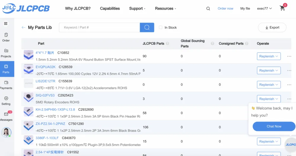
Fig. 1: A fragment of the component list from the JLCPCB library. The screenshot shows an example of the selection: some items (e.g., the LIS2DE12TR sensor or connectors) are available in stock with a specified LCSC code. For complex chips (like STM32F407), it shows 0 availability—meaning the part is not in the basic catalog. For such items, we marked the "Global Part" option, which will allow JLCPCB to source the required number of STM32F407 (minimum batch 5–6 pieces) specifically for our order. Thus, critical chips were included in the specification, even though they were not stocked at JLCPCB.
It should be noted that using Global Parts increases cost and time. In our case, the microcontroller and one of the sensors were sourced as Global (delivery 9–15 days), while everything else came from the standard range. We also verified that all components' packages were compatible with automated assembly (for JLCPCB, these are usually SMD components; our key chips are in LQFP, QFN packages, with small components like 0603, 0805 resistors, etc., which are suitable).
We had to buy many components for personal stock because while some parts were being processed, others ran out. In general, the component ordering process is very dynamic—every day you check what has run out and needs replacing, find a replacement, and place a MOQ order. It's interesting how through JLCPCB, you can order components directly from a wide range of vendors (such as Texas Instruments).
Placing an order on JLCPCB
When all the files are ready and components are defined, we placed the order through the JLCPCB website. The process looks like this:
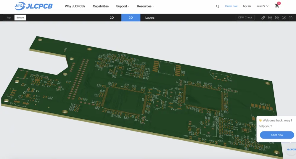
Gerber upload: On the PCB order landing page, we upload a zip with the Gerber files. The system shows a preview of the board and determines its size. We ensured the dimensions are correct, and the board is single-sided (most components on the top side).
Board settings: We select the quantity (we ordered 5 pieces, the minimum), thickness (1.6 mm standard), mask color (blue in our case), and board type (standard FR4).
Assembly: We indicate that component assembly is required. We choose the side for the assembly (Top side). The number of boards for assembly is specified – we selected 2 out of 5 (we immediately needed 2 assembled pieces, and the remaining 3 were reserved as clean spare boards).
BOM and CPL upload: Next, the system asks to upload the BOM and CPL files. We uploaded the prepared CSV files. The interface showed a list of components and their status (matches with the library, quantity, etc.).
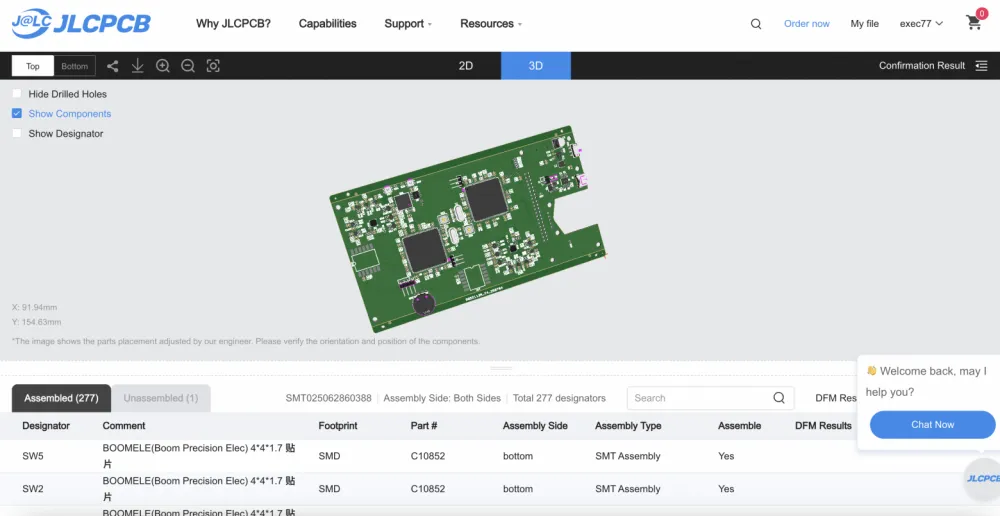
Fig. 2: JLCPCB interface after uploading BOM/CPL. It is visible that the system recognized 9 items as standard (LCSC) and 2 items as Global. The quantities of components are also shown (for the 2 assembled boards, plus reserves, totaling 12 STM32, sensor, and others were reserved). We checked each line: whether the identifier is correct, if it was automatically replaced by another. If necessary, a manual replacement can be chosen from the list (for example, if the recommended equivalent is unsuitable).
DFM check: Before final confirmation, the order undergoes an automatic check for manufacturing readiness (Design for Manufacturing). JLCPCB generated a report, warning about a couple of things: whether all components physically fit, if there are any conflicts. In our case, there were no critical issues – the board was designed according to their requirements.
Confirmation and payment: After the check and component selection, we confirmed the order. The cost was automatically calculated (detailed below). Payment was made online, with delivery selection (we chose economical shipping to Russia, around 2 weeks of waiting).
It is worth noting that JLCPCB also allows you to order only PCBs without assembly, but for our prototype, it is more convenient to receive the fully assembled modules right away.
During the check, you need to pay close attention to the orientation of the pin legs. It is not critical if the pins are above other components – this is allowed.
Cost and delivery time
Now let's review how the final cost was calculated and how long the whole process took.
Fig. 3: Cost breakdown of PCB + PCBA order. In the screenshot – the results of our order:
PCB Prototype (5 pcs): this is the price for the boards themselves (5 pieces, 2-layer, 100x60 mm, standard parameters).
Assembly (2 pcs): this includes the work on installation (installation + fixed fee for the batch), as well as the cost of all components. The largest contributions came from the STM32F4 (expensive, plus x2 pcs + spare), the sensor module, connectors, and other chips.
Customization: in this section, I selected many different options to see what the guys can actually do – there are even flexible PCBs available.
Shipping: very inexpensive, regular SF shipping within China was chosen.
VAT: What would it be without it.
Taking into account all expenses (MOQ, stock, overheads), the amount grew to $3500, and the device turned out to be much more expensive than anticipated, since the direct costs of its prototyping alone exceeded 300,000 rubles.
As it turned out, assembly costs more than the boards themselves, especially due to the specific components. If all parts were from the basic library, the price would have been lower. For example, global components added about $1000 to the cost (including the redundant 6 STM32, of which only 2 were soldered, the others as spares). Nevertheless, for a prototype, the cost is quite acceptable, considering the time saved on manual assembly.
As for the timeline, here is what happened:
The release of the boards took 3 days (standard time).
Purchase of Global Parts – about a week.
Assembly after receiving all components – 4–5 days.
Shipping to Russia – ~10 days.
In total, from payment to receiving, it took about 3 weeks. This is a bit longer than just the boards, but still quite good considering the individual chip procurement.
Results: Finished boards and testing
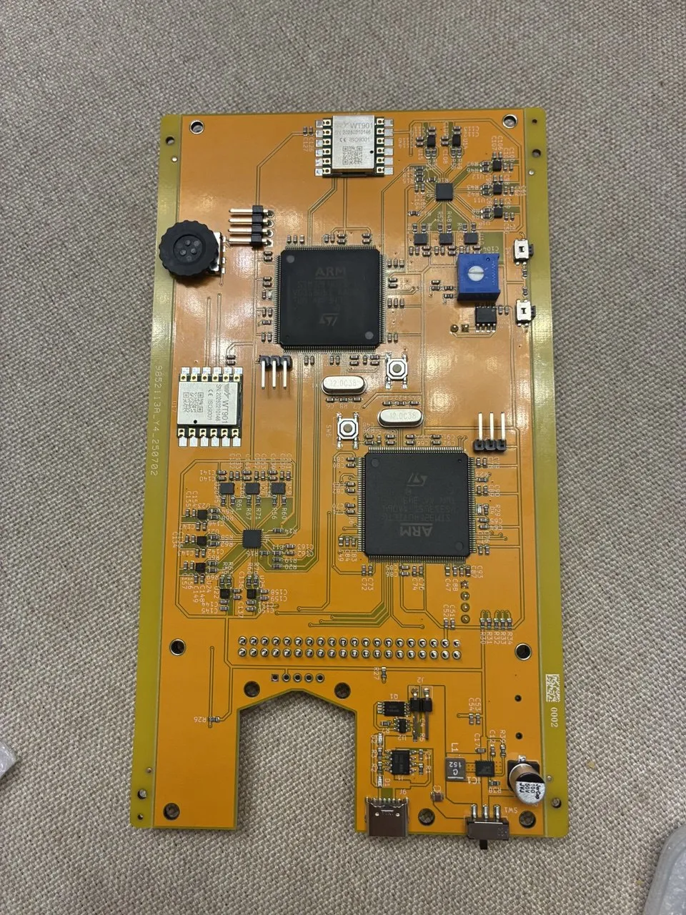
After about 3 weeks, we received the package from JLCPCB. Inside were sealed anti-static bags with our boards. Two boards were fully assembled, while the other three were just the printed circuit boards without components (this is how we ordered them).
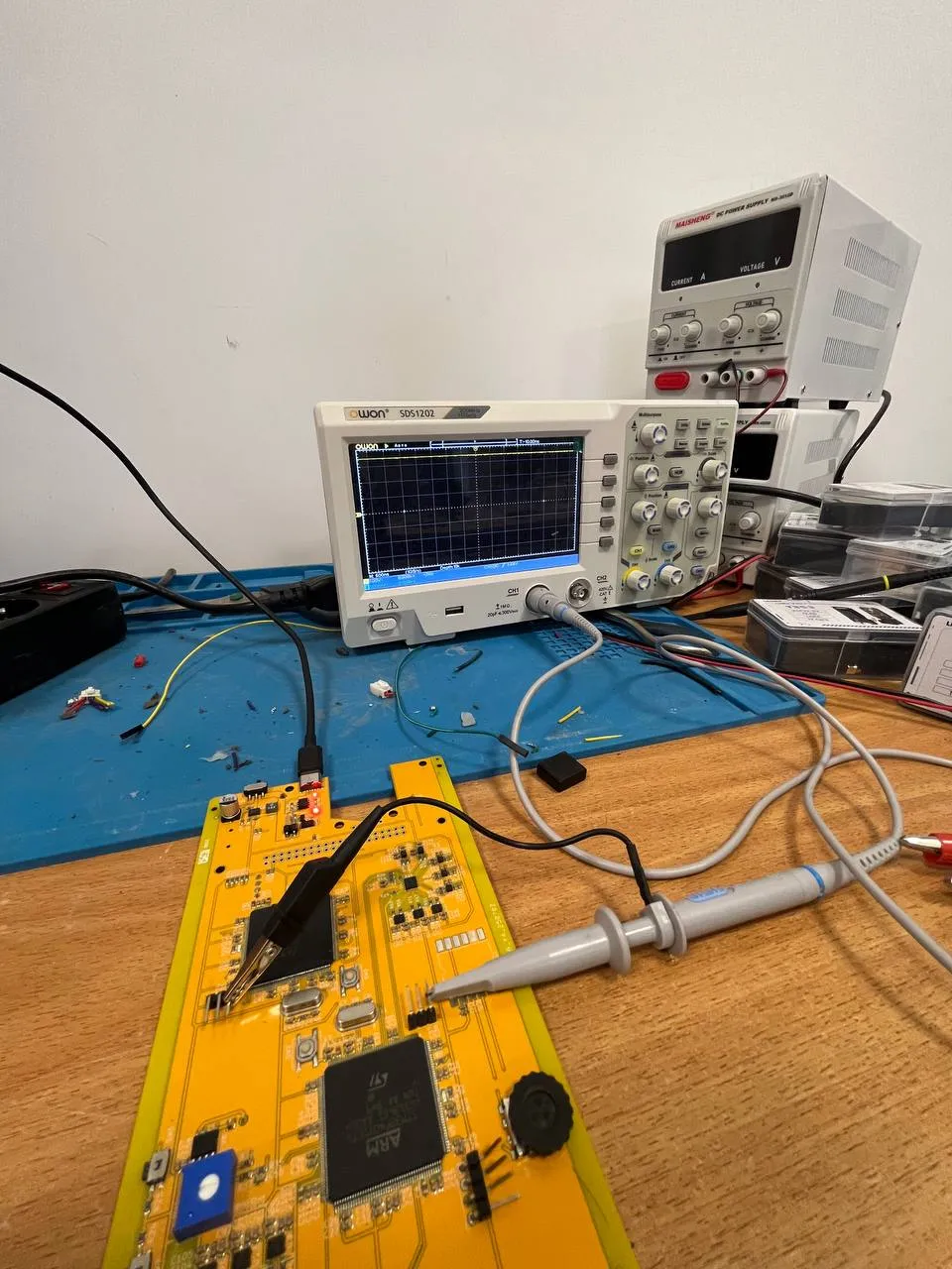
A visual inspection showed that the assembly was done neatly: all chips were placed correctly, the soldering was without bridges or cold joints, and the small resistors and capacitors were in place. The connectors and larger components were also correctly installed. We selected the board and connected the power – the device powered up on the first try, the microcontroller was flashed and gave the first telemetry data via UART. This indicates that the assembly quality is good and the components are intact.
Of course, after receiving, we conducted functional testing: we checked communication with sensors, power operation, and the computational part. In one of the next articles, we will describe the testing results in detail. But already at the acceptance stage, it was clear that the cooperation with JLCPCB was justified – we received professionally made boards in a short time, which allowed us to focus on the software and algorithmic part.
Conclusions: PCB printing and assembly through the JLCPCB service turned out to be convenient for our DIY project. Despite some difficulties with the component base (we had to place a global order for key chips), the final result—working devices—was worth the money spent. In this guide, we went through all the steps, from preparing the Gerber/BOM files to receiving the device, which we hope will be useful to those planning to order their electronics through similar services.
And of course, it’s worth mentioning alternatives in Russia—we have several services somewhat similar to the Chinese JLCPCB, with differences in component availability, production time, and a set of additional customization options.
In the next article, we’ll talk about choosing power supply elements, the display, UI, and interaction methods using a custom 3-axis joystick.


Write comment