- Hardware
- A
Z-80 4-bit ALU: Here's How It Works
When we write code for a microcontroller, behind the familiar instructions of the compiler lies a specific logic - registers, ALU, interrupts, buses, and timings that operate under their own rules.
The 8-bit Z-80 processor is famous for being used in many early personal computers, such as the Osborne 1, TRS-80, and Sinclair ZX Spectrum, and it is still applied in embedded systems and graphing calculators from Texas Instruments (TI). I always thought that the ALU (arithmetic logic unit) in the Z-80 had an 8-bit width, like almost any other 8-bit processor. But during reverse engineering the Z-80, I was surprised to discover that its ALU is only 4 bits wide! The founders of Zilog mentioned the 4-bit ALU in a very interesting conversation at the Computer History Museum, so it's not exactly a secret, but it wouldn't be called a well-known fact either.
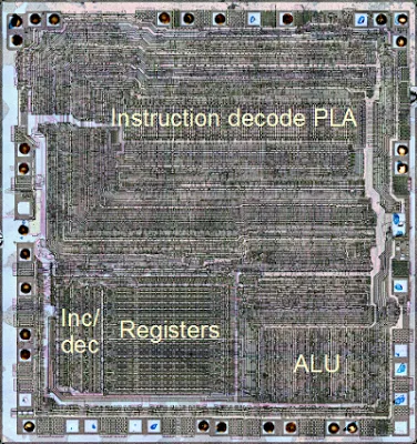
I am reverse engineering the Z-80 processor using images from the Visual 6502 project. The illustration below shows the overall structure of the Z-80 chip and the location of the ALU. The rest of the article goes into detail about the ALU: its architecture, how it works, and how exactly it is implemented.
I created the following block diagram to give an overview of the structure of the Z-80 ALU. Unlike Z-80 block diagrams published elsewhere, this diagram is based on the actual topology of the chip. The ALU consists of 4 one-bit cells that are "combined" into a 4-bit ALU. On the left side of the diagram, the register bus connects the ALU to the register file and the rest of the processor.
The operation of the ALU begins with loading two 8-bit operands from registers into internal latches. Then the ALU performs computation on the lower 4 bits of the operands and stores the result in the internal latches. After that, the ALU processes the upper 4 bits of the operands. Finally, the ALU writes all 8 bits of the result (the 4 lower bits from the latch and the 4 upper bits just computed) back to the registers. Thus, by performing two computation cycles, the ALU is capable of processing all 8 bits of data. ("Full 8 bits" may not sound impressive if you're reading this on a 64-bit processor, but it was quite sufficient for the time.)
As can be seen from the flowchart, the ALU has two internal 4-bit buses connected to an 8-bit register bus: the lower bus provides access to bits 0, 1, 2, and 3 of the registers, while the upper bus provides access to bits 4, 5, 6, and 7. The ALU uses latches to store operands until it can process them. The op1 latches store the first operand, while the op2 latches store the second. Each operand has 4 bits in the "lower" latch and 4 bits in the "upper" latch to hold all 8 bits.
The multiplexers select which data is used for the computation. The op1 latches are connected to a multiplexer that selects either the lower or the upper four bits. The op2 latches are connected to a multiplexer that selects either the lower or the upper four bits, and also allows the choice of either the original value or the inverted one. The inverted value is used for subtraction, negation, and comparison.
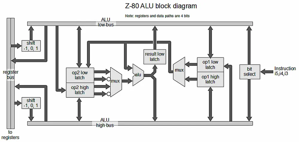
The two operands enter the “ALU core,” where the required operation is performed: addition, logical AND, logical OR, or logical exclusive OR (XOR). First, the ALU performs the computation on the lower bits and stores the 4-bit result in the lower result latch. Then, the ALU performs the second computation on the upper bits, writing the saved lower result and the newly computed upper bits onto the bus. The carry from the first computation is used in the second computation if necessary.
The Z-80 has advanced bit-addressable operations that allow setting, clearing, or checking a specific bit in a byte. In a bit-addressable operation, bits 5, 4, and 3 of the instruction select which of the 8 bits to use. At the far right of the ALU flowchart is a bit selection scheme that supports these operations. In this scheme, simple logic elements select one of the eight bits based on the command. The 8-bit value is written to the ALU bus, where it is used for the bit-addressable operation. Thus, the decoding of this part of the command occurs directly in the ALU, rather than in the usual instruction decoding logic.
The shift scheme in the Z-80 is also interesting. The 6502 and 8085 have a separate ALU operation for shifting right, while they perform left shifts by adding the number to itself. The Z-80, unlike them, performs the shift during the loading of the value into the ALU. When the Z-80 reads a value from the register bus, the shift scheme selects which lines of the register bus to use. It loads the value unchanged, with a left shift of one bit, or with a right shift of one bit. The bits "pushed in" at positions 0 and 7 are processed separately, as they depend on the specific instruction.
The block diagram also shows the path from the lower bus to the upper latches op2 and from the upper bus to the lower latches op1. This is necessary for the 4-bit BCD rotations RRD and RLD, which rotate a 4-bit digit in the accumulator along with two digits in memory.
The block diagram does not show simple circuits for calculating parity, checking for zero, and checking that a 4-bit value is less than 10. These values are used to set status flags.
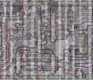
Crystal implementing the ALU
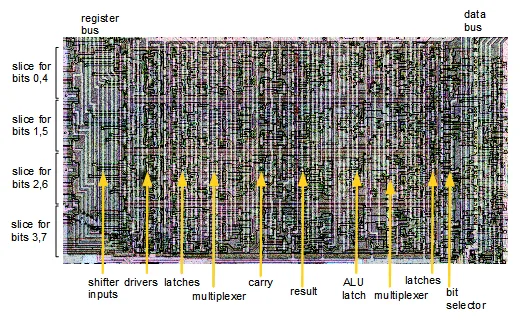
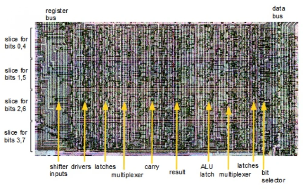
The illustration above shows an enlarged fragment of the ALU area on the Z-80 chip. Four horizontal "sections" are visible. The organization of each layer roughly corresponds to the block diagram. On the left, the register bus can be seen running vertically; the inputs of the shifter protrude from the ALU like "fingers" to grab the necessary bits. On the right, the data bus is also running vertically. The horizontal lines ALU low and ALU high are visible at the top and bottom of each layer. Yellow arrows indicate the location of some ALU components in one of the layers, but separate ALU circuits are indistinguishable at this scale.
Basic computational scheme of the ALU
The heart of each bit of the ALU is a circuit that computes the sum, AND, OR, or XOR bit for two single-bit operands. Upon zooming in, one can see the silicon on which this circuit is implemented; at this scale, transistors and connections that make up the logic elements are already distinguishable. Power, ground, and control lines are made of vertical metallic traces. The shiny horizontal stripes are polysilicon "conductors": they form connections in the circuit as well as the transistors themselves. I understand that it looks like mysterious gray lines, but if you analyze the image methodically, you can reconstruct the original circuit. The circuit is illustrated in the diagram below.
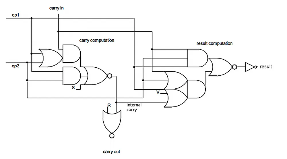
The circuit takes two operands (op1 and op2) and an input carry. It performs the operation (chosen by control lines R, S, and V) and forms the internal carry, output carry, and result.
Details on Calculation Logic in the ALU
The first step is "carry calculation." It is performed by one large multi-level logic element. It takes two bits of the operands (op1 and op2) and the input carry and computes the (inverted) internal carry that occurs when adding op1 + op2 + the input carry. A carry in such a sum can arise in only two ways: if both op1 and op2 are equal to 1 (the lower AND element) or if there is an input carry and at least one of the operands is equal to 1 (the upper elements). These two cases are combined by a NOR gate, which outputs the (inverted) internal carry. Then the internal carry is inverted by the lower NOR gate, forming the output carry, which becomes the input carry for the next bit. There are a couple of control lines that slightly complicate the carry formation. If S = 1, the internal carry is forced to be 0. If R = 1, the output carry is forced to be 0 (and thus the input carry for the next bit).
The multi-level result computation element is interesting because it outputs SUM, XOR, AND, or OR. It takes some effort to go through all the options, but if anyone needs details:
SUM: if R = 0, S = 0 and V = 0, the circuit forms the least significant bit of the sum op1 + op2 + input carry, that is, op1 xor op2 xor input carry. This is seen as follows: the output equals 1 if all three signals op1, op2, and input carry are set, or if at least one of them is set while there is no internal carry (i.e., exactly one is set).XOR: if R = 1, S = 0 and V = 0, the circuit forms op1 xor op2. Here the logic is the same as in the previous case, but the input carry is 0 due to R.AND: if R = 0, S = 1 and V = 0, the circuit forms op1 and op2. First, note that the internal carry is forced to be 0, so the lower AND element can never activate. The input carry is forced to be 1, so the result is determined by the upper AND element.OR: if R = 1, S = 1 and V = 1, the circuit forms op1 or op2. The internal carry is forced to be 0 due to S, and the output carry (and thus the input carry) is forced to be 0 due to R. Therefore, the upper AND element is disabled, and the result is controlled by the three-input OR element.
Strangely enough, conceptually this is much simpler than the ALU 8085. However, it is harder to understand than the ALU 6502: there, simple logic elements compute AND, OR, SUM, and XOR in parallel, and then the desired result is selected using pass transistors.
Conclusion
The Z-80 ALU is noticeably different from the 6502 or 8085 ALUs. The most significant difference is that the 6502 and 8085 use 8-bit ALUs, while the Z-80 ALU is 4-bit. The Z-80 supports bit-addressable operations that the 6502 and 8085 do not have. BCD support in the Z-80 is more advanced than the "decimal correction" in the 8085 because the Z-80 can work with both addition and subtraction, whereas the 8085 can only handle addition. However, the 6502 has even more developed BCD support: it has a decimal mode flag and fast, patented BCD logic.
If you designed an ALU in university classes, it is interesting to compare the "academic" ALU with the highly optimized ALU used in a real chip. It is curious to see what simplifications and compromises are applied in real hardware.
I made a more detailed schematic of the Z-80 ALU: it expands the flowchart and basic schematic above and shows the logic elements and transistors that make up the ALU.
I hope this immersion in the Z-80 has convinced you that even with a 4-bit ALU, the Z-80 could still perform 8-bit operations. Your old TRS-80 did not deceive you.


![From Virtual Hands to AI for Survivalists: Curious Open Agent OSes [and One Hardware Project]](https://cdn.tekkix.com/imgs/2026/05/habrcom/big/ce0b1057616faed51cd8b9f3b2b9.webp)
Write comment