- DIY
- A
Adaptation of the Colorlight 5A-75B board for the examples of the "Digital Circuit Synthesis School"
More details about the School can be found on the website, here we will look in detail at the sequence of actions that allow you to adapt another board for debugging examples studied at the School
"I molded it from what was" or another use of a budget board with FPGA
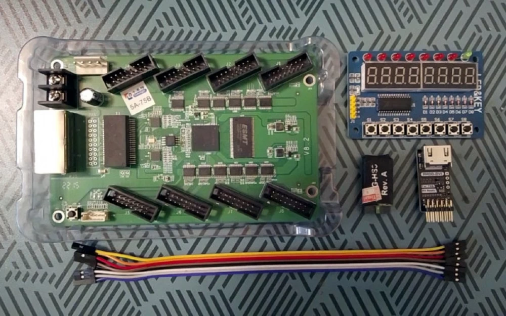
Colorlight 5A-75B is designed to control LED panels and is not a debug board in the usual sense of the term. Nevertheless, it has gained popularity among FPGA enthusiasts due to its availability, low cost (about 15$) and support for the Open Source design route based on Yosys.
Various versions of the board are known. I got version v8.2, which has:
-
Lattice FPGA ECP5 LFE5U-25F-6BG256C (25k LUT4)
-
Winbond 25Q32JVSIQ (32 Mbits SPI flash)
-
2x Realtek RTL8211FP Gigabit Ethernet PHYs
-
1x ESMT M12L64322A 2M 200MHz SDRAM (4 x 512k x 32bit)
-
12x 74HC245T (bus transceivers)
Detailed documentation for all components and pin descriptions can be found in the chubby75 repository. The Open Source route assembly with all the necessary software for synthesizing and simulating digital circuits is called OSS CAD. The latest versions of the assembly can be found on the Releases tab. Versions are updated daily. To configure the FPGA, the OSS CAD includes OpenFPGALoader and you can use any suitable JTAG adapter. You can see the list of all supported adapters with the command openFPGALoader --list-cables. I used my digilent_hs3.
The School repository contains examples and exercises on SystemVerilog, sequentially preparing students to solve real microarchitectural tasks. All examples can be run not only on the simulator but also on real FPGA layouts. The main elements of control and visualization of results on debugging boards are LEDs, seven-segment indicators, and buttons. In some examples, a monitor is used.
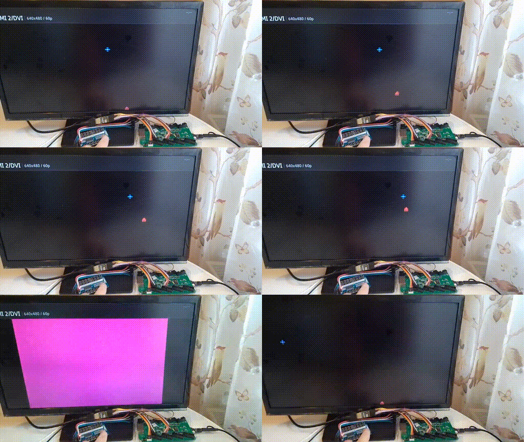
It is not possible to directly output an image from the Colorlight 5A-75B board to a monitor - it does not have the necessary connector, and it has to be purchased separately. There are two options here. Either use a VGA PMOD expansion board (costing about 10$) with a large number of pins, or an HDMI PMOD, which is cheaper, requires fewer wires for connection, but to form an HDMI stream, a higher frequency is used at which serializers (SerDes) operate. I chose the second option, connecting the HDMI PMOD expansion board (costing about 3$) that I had to the board simply using wires. The fpga4fun website has a good example that allows you to output an image from the FPGA layout to a monitor via the HDMI interface, which I used as a starting point.
There are 8 connectors ( J1 - J8 ) on the board for connecting LED panels, which can be controlled by the FPGA. Between the connectors and the FPGA itself, there are buffer chips configured to output data from the board. This imposes some limitations on the possibility of using J1-J8 for inputting data into the board, but this is not critical for HDMI. The table below shows the correspondence between the connector pin numbers and the FPGA ports to which I connected the HDMI PMOD. In this configuration, it was possible to display an image on the monitor with a resolution of 640x480 24bpp 60Hz.
|
FPGA |
J6-J7 |
Signal |
|---|---|---|
|
R15 |
J6.1 |
blue_p |
|
P13 |
J6.3 |
green_p |
|
N14 |
J6.6 Read also:
|
red_p |
|
G16 |
J7.1 |
clock_p |
|
T15 |
J6.2 |
blue_n |
|
P14 |
J6.5 |
green_n |
|
H15 |
J6.7 |
red_n |
|
H14 |
J7.2 |
clock_n |
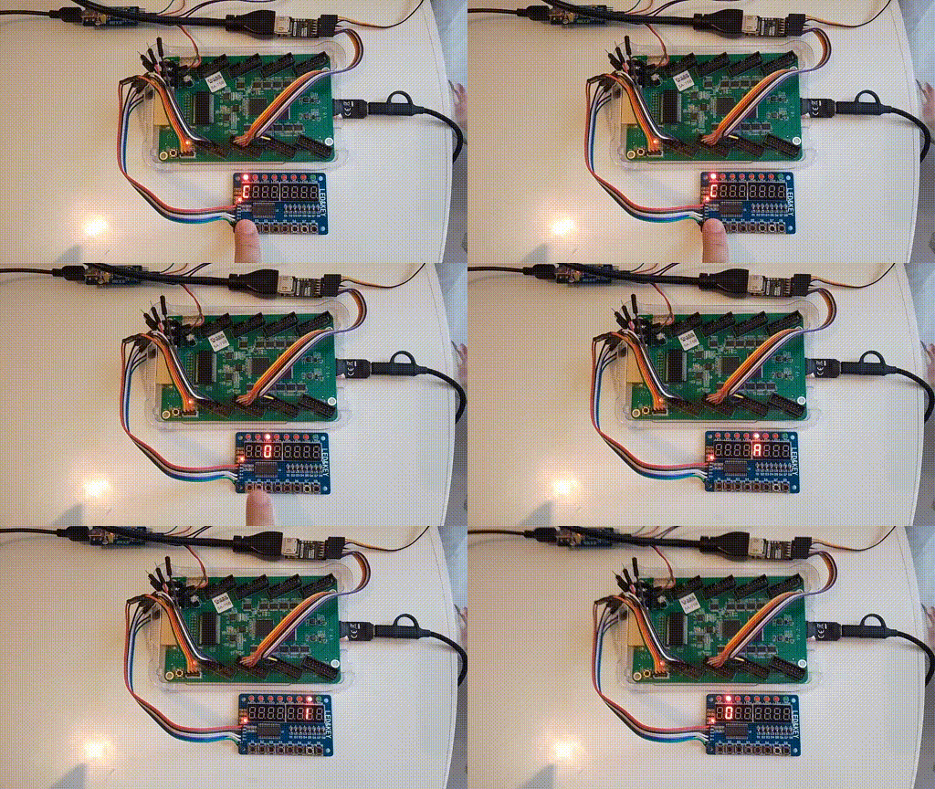
There is only one button and one LED on the board, which is clearly not enough. The School repository already supports an expansion board based on the TM1638 chip, which allows you to connect 8 LEDs, 8 seven-segment displays, and 8 buttons. The connection is made via a three-wire interface with signals stb, clk, dio (bidirectional) and ground gnd and power vcc circuits. A particular challenge is the connection of the bidirectional dio signal, as it cannot be routed to connectors J1 - J8, which are configured for output only. The solution is to use the J19 connector, which has a duplicate signal from the J28 button key+ (connected to the FPGA without a buffer), as well as gnd and 3v3. The remaining signals can be connected using the J5 connector. The table below shows the correspondence between the connector pin numbers and the FPGA ports to which the button and display block was connected.
|
FPGA |
J5, J19 |
Signal |
|---|---|---|
|
R7 |
J19.key+ |
dio |
|
J19.gnd |
gnd |
|
|
J19.3v3 |
vcc |
|
|
R12 |
J5.2 |
clk |
|
T14 |
J5.6 |
stb |
JTAG signals: TCK, TMS, TDI, TDO, Vref, GND are connected to pins J27, J31, J32, J30, J33, and J34 respectively. The easiest way to do this is from the back of the board. The 25MHz clock signal goes to the FPGA on port P5.
Connecting the power supply to the board is done through the J35 or J36 connectors, which are directly connected to the output buffers of the J1-J8 connectors. Thus, to ensure that the voltage on the J1-J8 connectors does not exceed the allowable values, it is necessary to use a 3.3V power source, not 5V.
In the configuration with PMOD HDMI and the TM1638 button and indication block, the Colorlight 5A-75B board is already a full-fledged budget debugging tool. Its separate advantage is the presence of two gigabit Ethernet ports and SDRAM, which is rarely found in entry-level debugging boards in the specified price range.
Adding support for Colorlight 5A-75B to the environment with examples from the Digital Circuit Synthesis School
I have not found a step-by-step guide on integrating new debugging boards into the project anywhere and decided to fill this gap:
-
Setting up the environment to support Lattice ECP5 FPGAs and OSS CAD is done using the
00_setup.source_bashand00_setup_yosys.source_bashscripts. A quick analysis showed that it is necessary to create a folder in theboardsdirectory of the main basics-graphics-music repository, the name of which must include the wordsyosysandecp5, then the scripts automatically add a new board when running the main environment setup scriptcheck_setup_and_choose_fpga_board.bash. -
Next, in this new folder, you need to create a wrapper file
board_specific_top.svthat connects the top level of the exampleslab_top.svto the specific board. Add a file to the folder that describes the binding of FPGA ports to specific signalsboard_specific.lpf. You can also add additional.svand.vfiles needed for proper operation - they will also be automatically added during synthesis. In my case, these were the HDMI controller fileshdmi.vand the clock generation blockclock.v. -
Add a makefile describing the synthesis and configuration of the FPGA. In my case, this is a call to
yosys,nextpnr-ecp5,ecppack, andopenFPGALoaderwith appropriate parameters.
Running examples on the board
To run the examples, you need to go to the folder with a specific lab work and run the script 03_synthesize_for_fpga.bash, which performs the synthesis of the sources and the configuration of the FPGA.
Examples are divided into several classes:
-
basics
-
graphics
-
music
-
microarchitecture
-
cpu
Due to the lack of an i2c microphone at hand, I was unable to test the 3_music examples on the board, but the 1_basics and 2_graphics examples worked successfully.
It should be noted that Yosys and Icarus Verilog have very limited support for SystemVerilog and some examples from microarchitecture did not run. This problem was solved with the help of the sv2v converter, which converts SystemVerilog code to Verilog HDL.
All source codes were handed over to the School organizers and will soon appear in the main repository.





Write comment