- DIY
- A
Ancient Technologies: ATAPI IDE, Part One, Preparatory
One day I wanted to build a PC no older than the first Pentium for DOS and WIN9x games. And I wanted to organize it not as just another huge box on the desk, but in the format of a regular TV console.
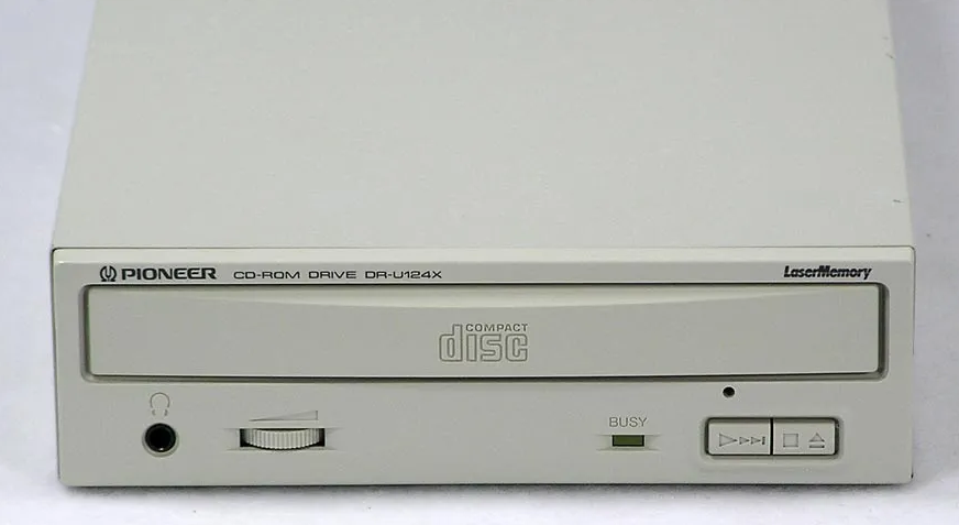
I found a Baby-AT motherboard, the so-called Super7, which is a motherboard for Socket-7 on steroids: it already has SDRAM memory, an AGP slot, and a large second-level cache. I found a case for mITX, where the Baby-AT can fit, and most importantly, the power supply is PicoPSU, which allows using a standard laptop power supply. For the HDD, I used an IDE SSD, which is quite cheap. While testing this setup on the desk, I used an IDE ATAPI optical drive. Everything worked great. The only issue is that the small mITX case doesn’t have space for a 5.25 drive, and I need the drive, because even for DOS, there were games with CD support, not to mention WI9x. And that’s when I realized - it’s time to make my own IDE ATAPI optical drive emulator, compact and silent. This will be the subject of this small series of articles, which I hope to bring to a logical conclusion. If you’re interested - join in, it’s more fun together!
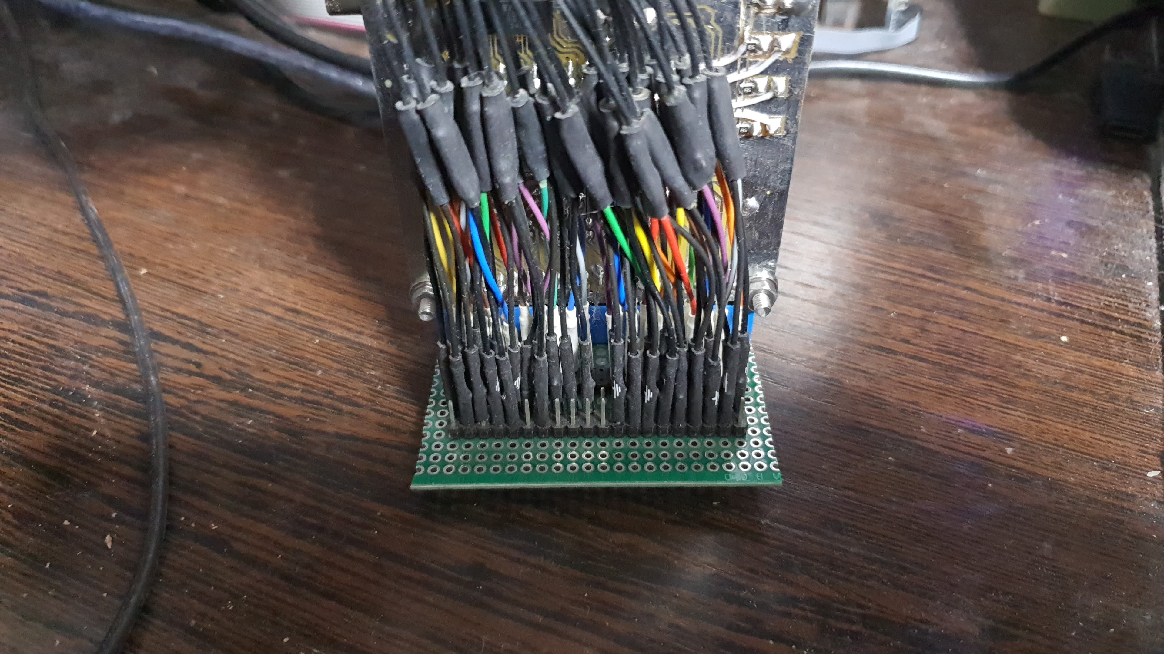
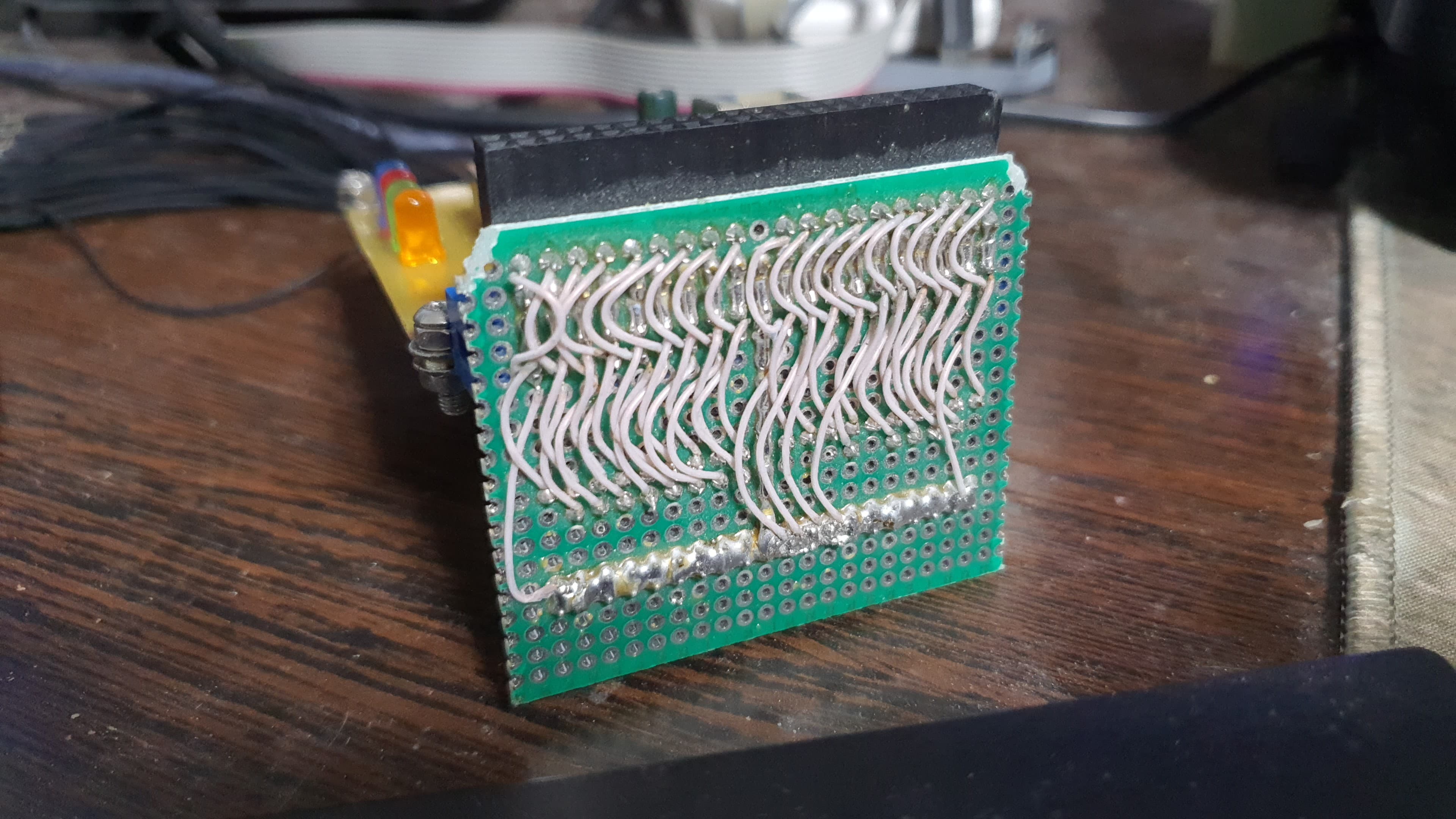
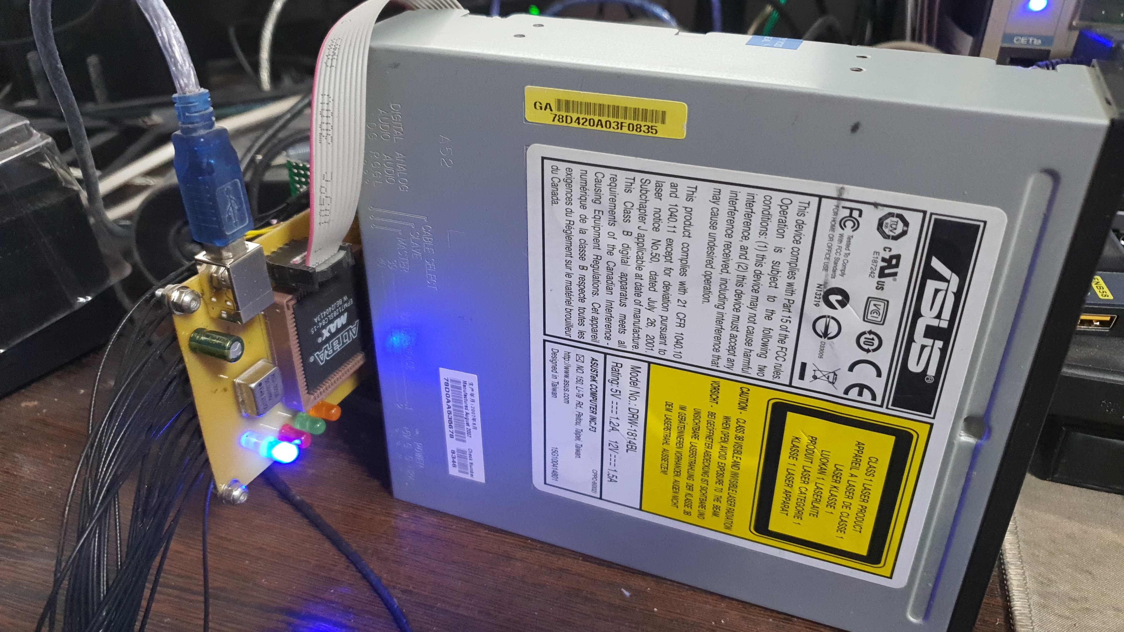
More photos under the spoiler.

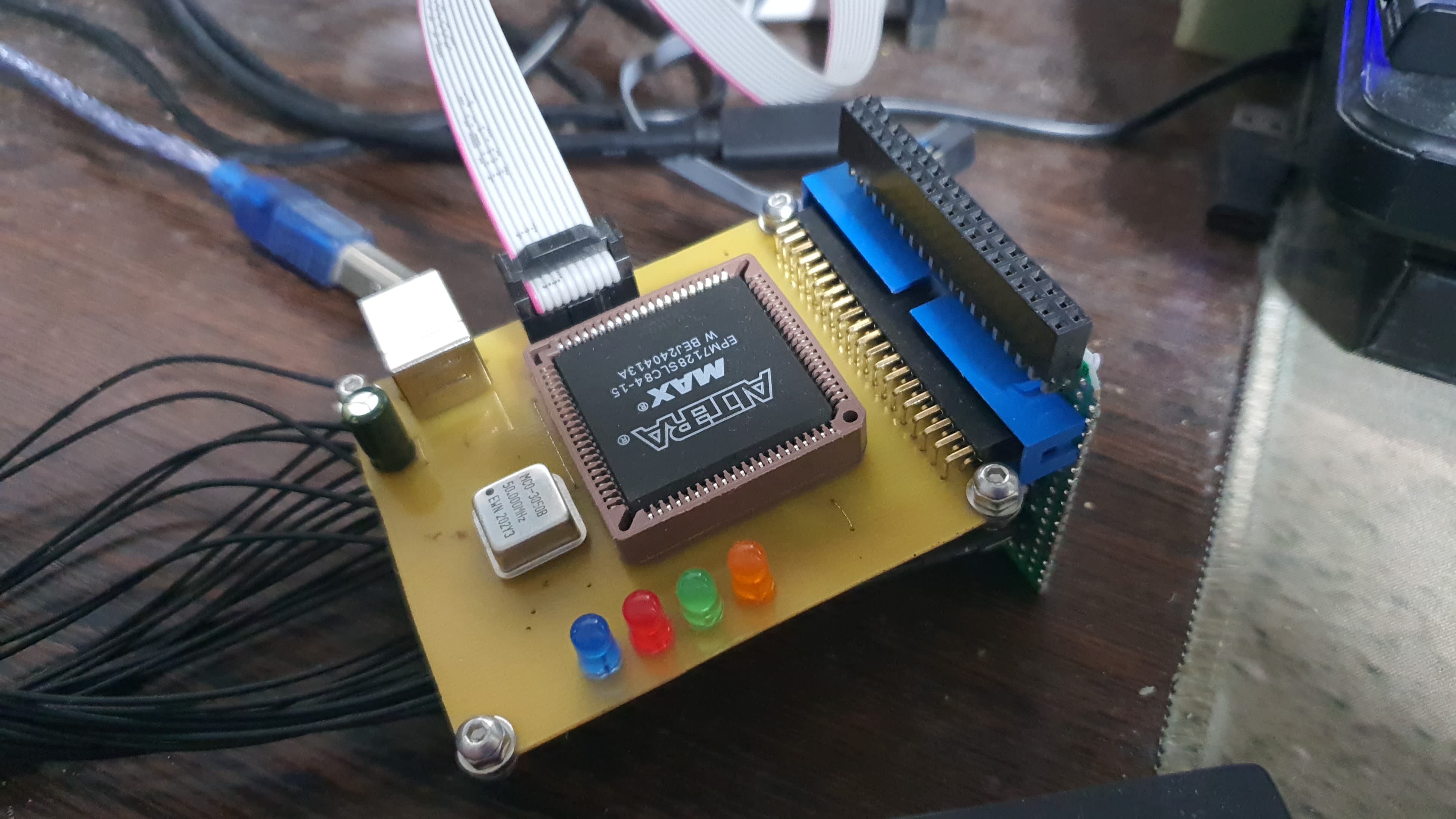
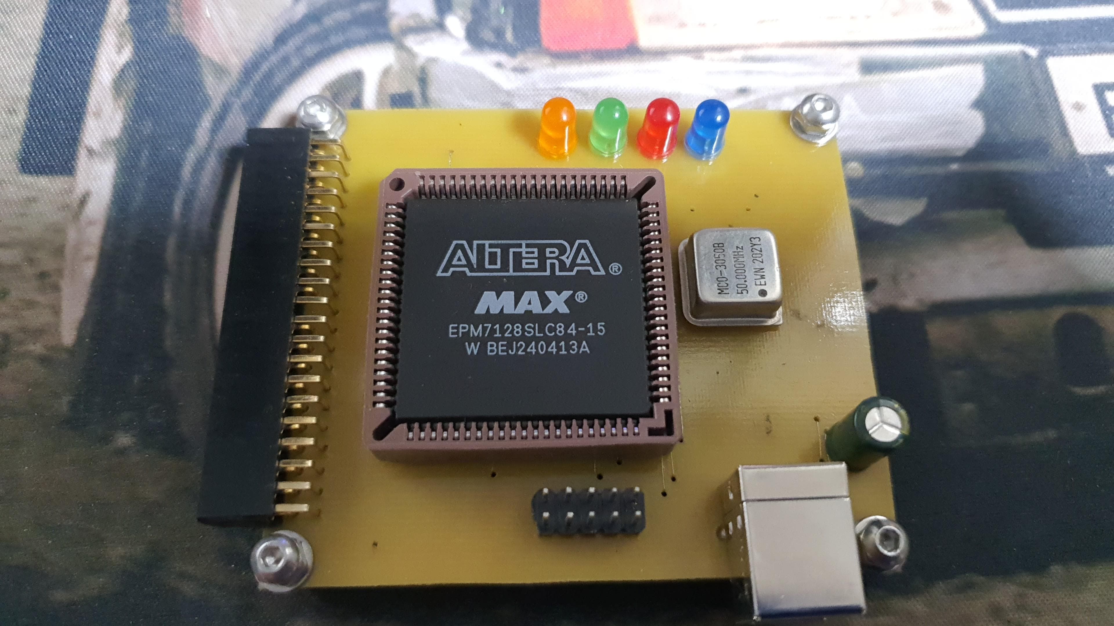
It’s time to describe the configuration for the CPLD. But first, a communication protocol needs to be developed. It’s obvious that the CPLD is too small to fit any microprocessor core, so it will just be a finite state machine. The protocol will be byte-based, but each byte will be a separate and recognizable command. After almost a week of thinking, trials, and errors (some options ran into the number of PIA connections in the CPLD, others into the number of registers), I came up with this command system:
0000 HHHH - WRITE HEX
0001 .AAA - WRITE REG CS1X
0010 .AAA - WRITE REG CS3X
0011 .... - WRITE DMA
0100 0CRA - SET {CSEL, RESET, DMACK}
0100 1... - READ STATUS
0101 .AAA - READ REG CS1X
0110 .AAA - READ REG CS3X
0111 .... - READ DMA
1.WW WWWW - IDE TIMING
These are the commands sent to the device. Most of them do not require a response. As you can see, the high nibble is the command itself, and the low nibble is its modifier. Command 0x is the transfer of a parameter in hex, i.e. from 0x00 to 0x0F it’s essentially transferring a nibble from 0x0 to 0xF. The device has a 16-bit parameter register, which shifts by a nibble to the left with each such command, and the lower nibble gets a new value. So, to write a byte, you need to send 2 commands, and if you need to write a word, it’s 4. By accumulating the necessary parameter, you can issue the write command, and the data from the parameter register will go to the IDE bus. It’s like G-code in reverse. The IDE TIMING command allows setting the data strobe width in 20ns steps. Read commands initiate the return of data to the PC. The response format is the same:
0000 HHHH - READ HEX
0101 .AAA - REG CS1X ACK
0110 .AAA - REG CS3X ACK
0111 .... - READ DMA
1..R PDQI - READ STATE {RESRV, PDIAG, DASP, DMARQ, INTRQ}
So, if this was a register read, all the necessary nibbles will be received first, and then the actual opcode will arrive as confirmation. So parsing the return stream is just as simple as forming the outgoing one. And since for Windows there's the D2XXX library from the chip manufacturer, which allows forming a large block of data, the USB overhead becomes insignificant. For example, to read 256 words of the data register (1 sector is 512 bytes), it's enough to send 256 opcodes at once, and they will be cached by the driver and the chip itself, so you just have to wait for the same size block of responses.
Now let's move on to configuration.
Full Verilog code.
//
module IDE_DIRECT(
	// System
	input		CLK,				// 50MHz clock
	// LEDs
	output		reg LED_WR,			// USB write LED
	output		reg LED_RD,			// USB read LED
	output		reg LED_ACT,		// Active drive LED
	// FTDI bus
	inout		[7:0]FD,			// Data bus
	output		reg nRD,			// Read strobe
	output		reg WR,				// Write strobe
	input		nRXF,				// Data present flag
	input		nTXE,				// Transmitter ready flag
	// IDE bus
	inout		[15:0]DD,			// IDE data bus
	output		reg [2:0]DA,		// Address bus
	output		reg CS1X,			// Primary registers
	output		reg CS3X,			// Additional registers
	output		reg DIOR,			// Read signal
	output		reg DIOW,			// Write signal
	output		reg RESET,			// Reset signal
	inout		CSEL,				// Cable select signal
	input		IORDY,				// Ready signal
	input		INTRQ,				// Interrupt request signal
	input		DMARQ,				// DMA request signal
	output		reg DMACK,			// DMA acknowledge signal
	input		DASP,				//
	input		PDIAG,				//
	inout		RESERV				// Reserved
);

// Stubs
assign RESERV = 1'bZ;

// Signal setup
assign CSEL = (CSELR)? 1'b0 : 1'bZ;

// Buses
assign FD[7:0] = (~WR) ? 8'hZZ : (STATUS[1]) ? {3'h4,RESERV,PDIAG,DASP,DMARQ,INTRQ} : (STATUS[0]) ? Answer[7:0] : 8'h00;
assign DD[7:0] = (~DIOW) ? Param[7:0] : 8'hZZ;
assign DD[15:8] = (~DIOW & ~DA[2] & ~DA[1] & ~DA[0]) ? Param[15:8] : 8'hZZ;

// USB -> IDE
// 0000 HHHH - WRITE HEX
// 0001 .AAA - WRITE REG CS1X
// 0010 .AAA - WRITE REG CS3X
// 0011 .... - WRITE DMA
// 0100 0CRA - WRITE {CSEL, RESET, DMACK}
// 0100 1... - READ STATUS
// 0101 .AAA - READ REG CS1X
// 0110 .AAA - READ REG CS3X
// 0111 .... - READ DMA
// 1.WW WWWW - IDE TIMING

// IDE -> USB
// 0000 HHHH - READ HEX
// 0101 .AAA - REG CS1X ACK
// 0110 .AAA - REG CS3X ACK
// 0111 .... - READ DMA
// 1..R PDQI - READ STATE {RESRV, PDIAG, DASP, DMARQ, INTRQ}

// Multiplexer of output data
wire [7:0]Answer;

assign Answer[7:0] = (SendCnt[2]) ? {4'h0,DR[15:12]}
						:
						(SendCnt[1]) ?
							(SendCnt[0]) ? {4'h0,DR[11:8]} : {4'h0,DR[7:4]}
							:
							(SendCnt[0]) ? {4'h0,DR[3:0]} : OpCode[7:0];

// Selection signals
wire WriteHex;
wire WriteReg;
wire WriteDMA;
wire WriteCtrl;
wire ReadStat;
wire ReadReg;
wire ReadDMA;

assign WriteHex  = ~OpCode[7] & ~OpCode[6] & ~OpCode[5] & ~OpCode[4];
assign WriteReg  = ~OpCode[7] & ~OpCode[6] & (OpCode[5] ^  OpCode[4]);
assign WriteDMA  = ~OpCode[7] & ~OpCode[6] &  OpCode[5] &  OpCode[4];
assign WriteCtrl = ~OpCode[7] &  OpCode[6] & ~OpCode[5] & ~OpCode[4] & ~OpCode[3];
assign ReadStat  = ~OpCode[7] &  OpCode[6] & ~OpCode[5] & ~OpCode[4] &  OpCode[3];
assign ReadReg   = ~OpCode[7] &  OpCode[6] & (OpCode[5] ^  OpCode[4]);
assign ReadDMA   = ~OpCode[7] &  OpCode[6] &  OpCode[5] &  OpCode[4];

// Variables
reg nRXFr = 1'b1;					// Synchronization of nRXF signal
reg nTXEr = 1'b0;					// Synchronization of nTXE signal
reg IORDYr;							// Synchronization of IORDY signal
reg CSELR;							// Activate CSEL signal to ground OK
//
reg [1:0]SubCycle = 2'h0;			// Subcycle counter
reg [7:0]OpCode;					// Opcode from USB
reg [15:0]Param;					// Command parameter
reg [15:0]DR;						// IDE data register
reg [5:0]SetTime;					// Transaction length IDE
reg [5:0]IDETime;					// IDE transaction timer
reg [1:0]STATUS;					// Status transmission flag
reg [2:0]SendCnt;					// Number of data to send

// State machine description
reg [3:0]FState;					// State machine
localparam fsINIT    = 4'h0;		// Full initialization
localparam fsURXF    = 4'h1;		// Analyze RXF flag
localparam fsUREAD   = 4'h2;		// Read from USB
localparam fsEXECUTE = 4'h3;		// Execute opcode
localparam fsWPREP   = 4'h4;		// Prepare selected write
localparam fsWRITE   = 4'h5;		// Write transaction on IDE bus
localparam fsSTATUS  = 4'h6;		// Prepare status to send to USB
localparam fsUWRITE  = 4'h7;		// Write to USB
localparam fsUGAP    = 4'h8;		// Protected wait between writes
localparam fsRPREP   = 4'h9;		// Prepare for reading
localparam fsREAD    = 4'hA;		// Read transaction on IDE bus
localparam fsSEND    = 4'hB;		// Prepare to send data to USB

// Read opcode
always @(posedge nRD) begin
	// Save data on opcode read rising edge
	OpCode[7:0] <= FD[7:0];
end

// Read data from IDE
always @(posedge DIOR) begin
	DR[15:0] <= DD[15:0];
end

// Synchronous logic
always @(posedge CLK) begin
	// Synchronization of signals
	nRXFr <= nRXF;
	nTXEr <= nTXE;
	IORDYr <= IORDY;

	// LEDs
	LED_ACT <= DASP;
	LED_RD <= nRXF;
	LED_WR <= ~nTXE;

	// Subcycle counter
	SubCycle[1:0] <=  {SubCycle[0] & ((FState == fsUREAD) | (FState == fsUWRITE) | (FState == fsUGAP)),~SubCycle[1] & ((FState == fsUREAD) | (FState == fsUWRITE) | (FState == fsUGAP))};

	// State machine
	case (FState[3:0])
		// Init
		fsINIT : begin
					// Init all variables
					nRD <= 1'b1; WR <= 1'b0;
					DA[2:0] <= 3'h0; CS1X <= 1'b0; CS3X <= 1'b0;
					DIOR <= 1'b1; DIOW <= 1'b1;
					CSELR <= 1'b0; RESET <= 1'b0; DMACK <= 1'b1;
					// Reset flags
					STATUS <= 1'b0;
					// Begin work
					FState <= fsURXF;
				end
		// Check if data present in USB
		fsURXF : if (~nRXFr) FState <= fsUREAD; else FState <= fsURXF;
		// Read USB
		fsUREAD : begin
					// Read signal
					nRD <= SubCycle[1] & ~SubCycle[0];
					// Done
					if (SubCycle[1] & ~SubCycle[0]) FState <= fsEXECUTE;
					end
		// Execute opcode
		fsEXECUTE : begin
						// Is it timing setup?
						if (OpCode[7]) SetTime[5:0] <= OpCode[5:0]; else
							// Is it HEX?
							if (WriteHex) Param[15:0] <= {Param[11:0],OpCode[3:0]}; else
								// Is it control signals?
								if (WriteCtrl) {CSELR,RESET,DMACK} <= OpCode[2:0];
						// Write to IDE
						if (WriteReg | WriteDMA) FState <= fsWPREP; else
						// Read input state
						if (ReadStat) FState <= fsSTATUS; else
						// Read from IDE
						if (ReadReg | ReadDMA) FState <= fsRPREP; else
						// Otherwise back to idle
						FState <= fsURXF;
						end
		// Prepare to write to IDE
		fsWPREP: begin
					// PIO settings
					if (WriteReg) {DMACK,CS1X,CS3X,DA[2:0]} <= {1'b1,OpCode[5:4],OpCode[2:0]};
					// DMA settings
					if (WriteDMA) {DMACK,CS1X,CS3X,DA[2:0]} <= 6'h18;
					// Set signals
					if (~WriteReg & ~WriteDMA) FState <= fsURXF; else
						// Proceed only if USB not busy
						if (~nTXEr) begin
							// Activate write
							IDETime[5:0] <= SetTime[5:0];
							DIOW <= 1'b0;
							FState <= fsWRITE;
							end
					end
		// IDE write transaction
		fsWRITE : if (IDETime[5:0] == 6'h00) begin
					// Turn off write
					DIOW <= 1'b1; DMACK <= 1'b1;
					// Exit
					FState <= fsURXF;
					end else if (IORDYr) IDETime[5:0] <= IDETime[5:0] - 6'h01;
		// Prepare status
		fsSTATUS : begin
					// Set status flag
					STATUS[1] <= 1'b1;
					FState <= fsUWRITE;
					end
		// Send to USB
		fsUWRITE : begin
					// Read signal
					WR <= ~(SubCycle[1] & ~SubCycle[0]);
					// Done
					if (SubCycle[1] & ~SubCycle[0]) begin
						// Sending status?
						if (STATUS[1]) begin
							STATUS[1] <= 1'b0;
							FState <= fsURXF;
							end else
							// Sending IDE data?
							if (STATUS[0]) begin
								// All done?
								if (~SendCnt[2] & ~SendCnt[1] & ~SendCnt[0]) begin
									// Clear status
									STATUS[0] <= 1'b0;
									// Exit
									FState <= fsURXF;
									end else FState <= fsUGAP;
								end
						end
					end
		//
		fsUGAP : if (SubCycle[1] & ~SubCycle[0] & ~nTXEr) begin
					// Count nibbles
					SendCnt[2:0] <= SendCnt[2:0] - 3'h1;
					// Return to write if USB free
					FState <= fsUWRITE;
					end
		// Prepare to read from IDE
		fsRPREP : begin
					// PIO settings
					if (ReadReg) {DMACK,CS1X,CS3X,DA[2:0]} <= {1'b1,OpCode[5:4],OpCode[2:0]};
					// DMA settings
					if (ReadDMA) {DMACK,CS1X,CS3X,DA[2:0]} <= 6'h18;
					// Set signals
					if (~ReadReg & ~ReadDMA) FState <= fsURXF;
						else begin
						// Activate write
						IDETime[5:0] <= SetTime[5:0];
						DIOR <= 1'b0;
						FState <= fsREAD;
						end
					end
		// IDE read transaction
		fsREAD : if (IDETime[5:0] == 6'h00) begin
					// Turn off write
					DIOR <= 1'b1; DMACK <= 1'b1;
					// Exit
					FState <= fsSEND;
					end else if (IORDYr) IDETime[5:0] <= IDETime[5:0] - 6'h01;
		// Prepare to send bytes to USB
		fsSEND : begin
					// Set status flag and amount to send
					STATUS[0] <= 1'b1;
					if (~DA[2] & ~DA[1] & ~DA[0]) SendCnt[2:0] <= 3'h4; else SendCnt[2:0] <= 3'h2;
					// If USB is free
					if (~nTXEr) FState <= fsUWRITE;
					end
	endcase
end

// End
endmodule
Quickly wrote a simple program to connect to the interface and checked the basic IDE commands:
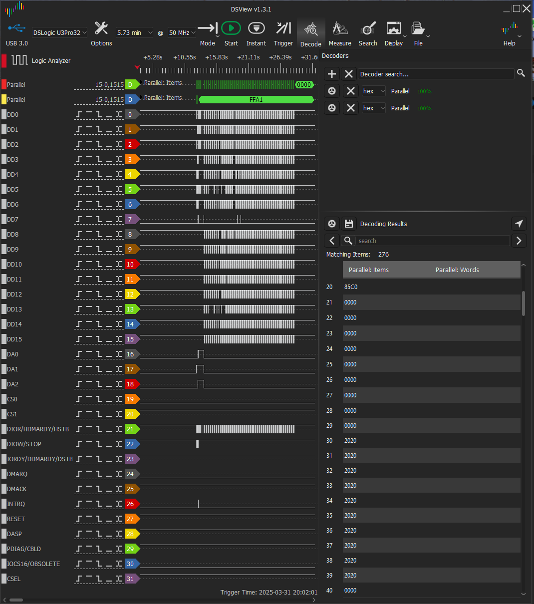
Looks like the concept actually works and the control program can be developed further to add all the necessary IDE ATA/ATAPI device management functions. This device is not for high-speed data transfer, but it does allow you to get data from different IDE devices. You can even connect an HDD. In theory, you could even make a passive adapter to ISA and connect an ESDI controller with an MFM HDD like the ST-225.
That's all for today. Next time, we'll be looking at ATAPI commands and discussing the block diagram for the future optical disc emulator. Thanks for your attention.


Write comment