- DIY
- A
Amplifier Class D on TPA3255
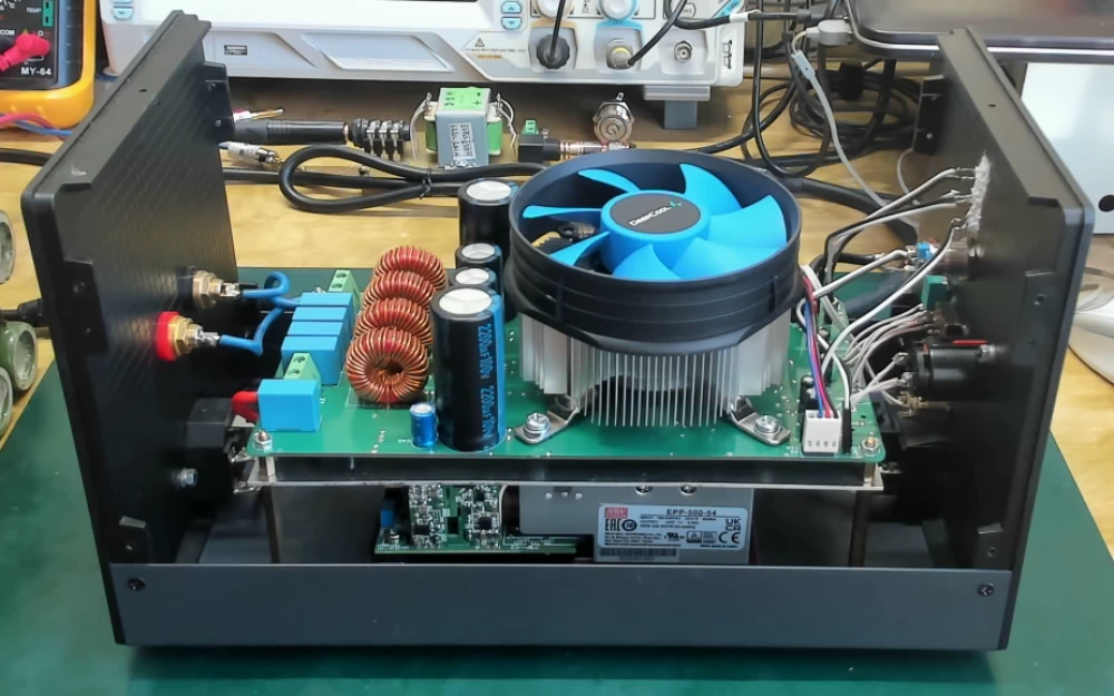
In this article, we will talk about a Class D amplifier based on the TPA3255 chip from Texas Instruments. The amplifier is made according to the parallel-bridge connection scheme to obtain maximum power. Let's look at it from all sides.
This article will discuss a class D amplifier based on the TPA3255 chip from Texas Instruments. The amplifier is made according to the parallel-bridge connection (PBTL) scheme to obtain maximum power. Let's look at it from all sides.
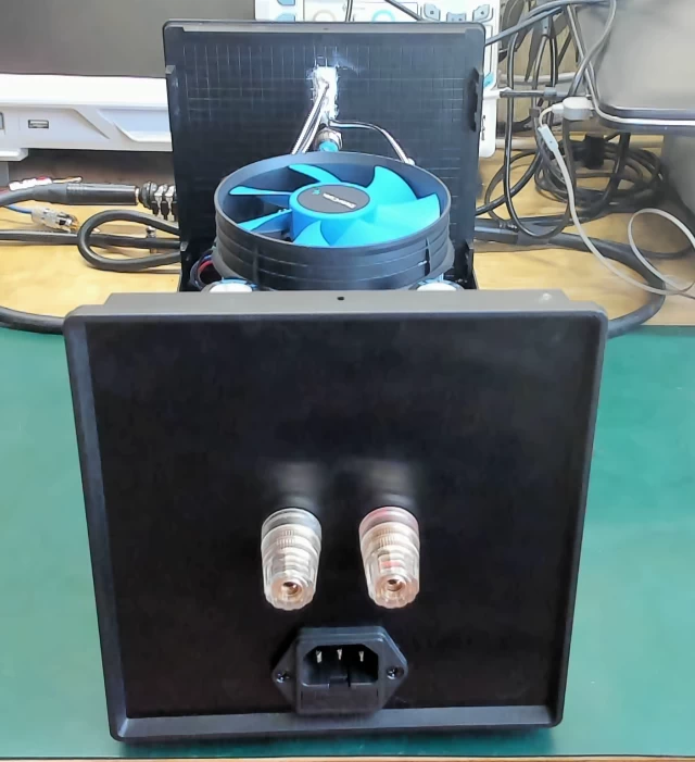
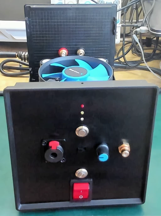
On the front panel, there is a power button, Reset, a balanced input for connecting a sound card, an unbalanced input for a smartphone or another source with a sensitivity of 0.1 Volts with a preamplifier Kus=10 and volume control, input switch. Forced cooling button, fan on indicators, thermal overload and emergency mode indicators.
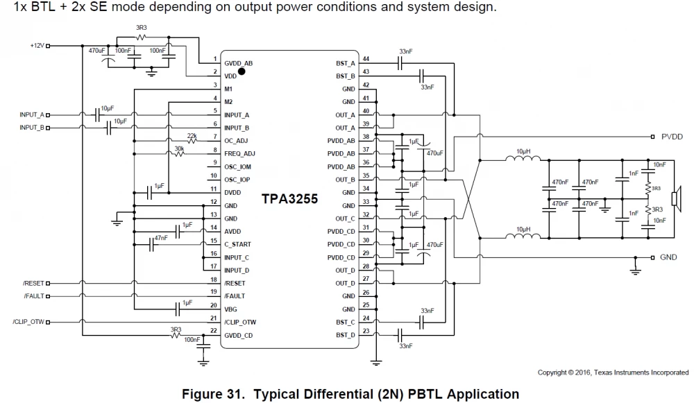
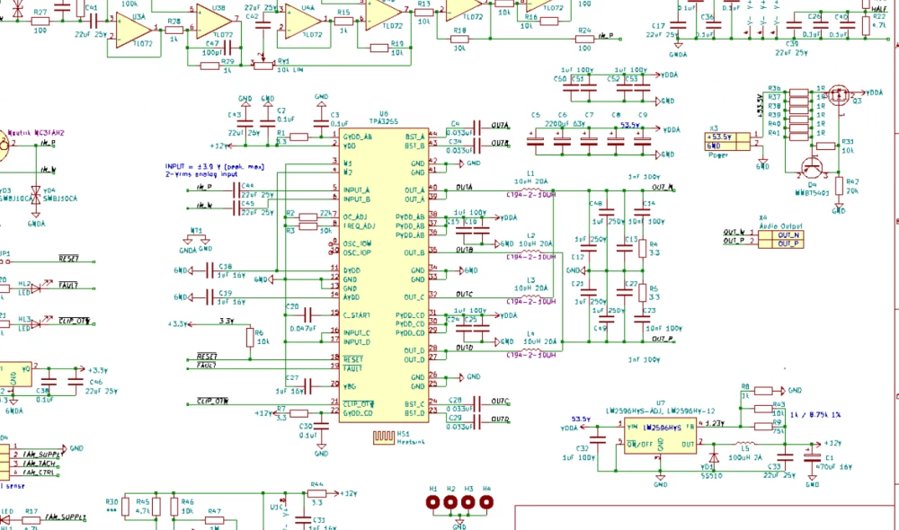
This project is based on the article "600W Audio Signal Amplifier / tekkix". Let's look at some important points. First of all, it should be noted that the author changed the output switching circuit of the chip. This is what the circuit looks like in the datasheet.
This is what the author's circuit looks like
An inductance is installed at each output. I left it as the author did, assuming that this solution is more correct - better carrier frequency filtering and less heating of the inductances.
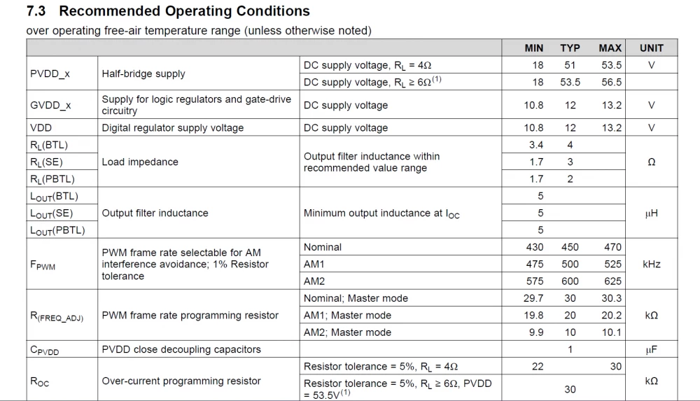
Next, the author claims that the supply voltage in his project is 53.5 Volts. This figure cost me 4 chips - after a few power-ups, the red emergency mode LED lit up. The chip just burned out.
And if we look at the datasheet, we will see that the voltage of 53.5 Volts for a 4 Ohm load is the maximum voltage, and the typical one is 51. At 51 Volts, the amplifier worked a little longer, then the same symptoms of chip death. That is, it was experimentally established that for a 4 Ohm load, the supply voltage of the amplifier should not exceed 50 volts. Now I have set it to 50 volts - the third week is normal.
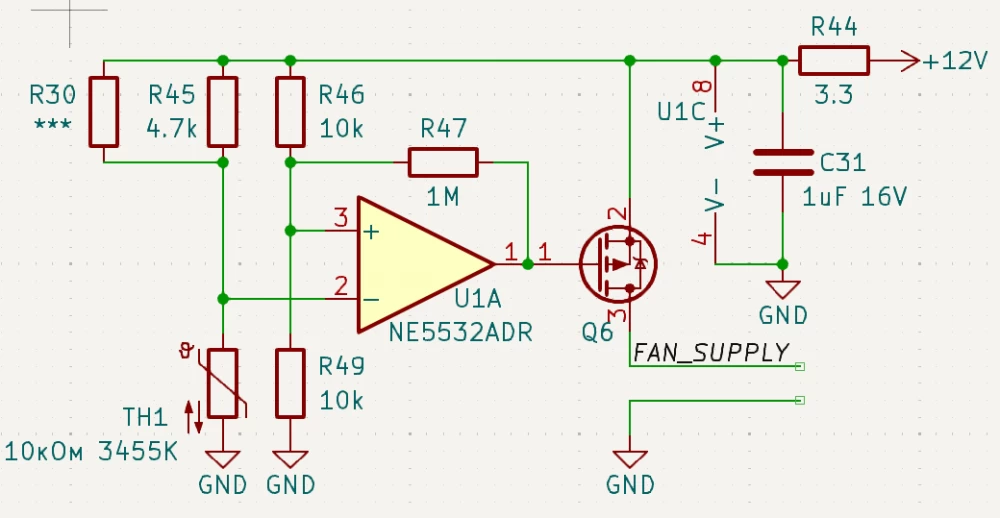
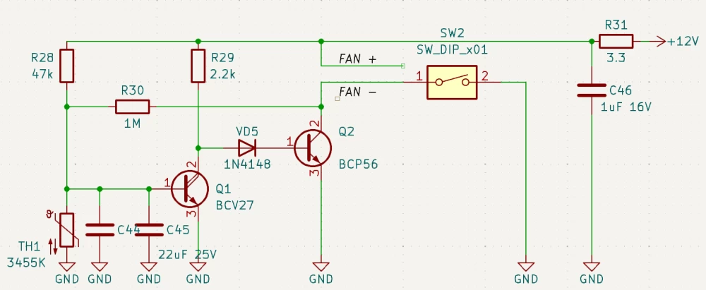
The fan control circuit of the chip was modified by me so that the rotation speed is proportional to the heating temperature. Here is the author's diagram
Here is my diagram
Now about the input signals. In the original circuit, the balanced input is connected to the output of the unbalanced input preamplifier.
And this is what happens — the balanced input signal is mixed with the output of the unbalanced input preamplifier, which leads to a signal attenuation by half (by ear) and strong distortions appear. Therefore, I inserted an input switch into the circuit and removed the protective bidirectional diodes to reduce the influence on the signals
And the last change — the power and signal grounds are separated by a 1.5 Ohm resistor.
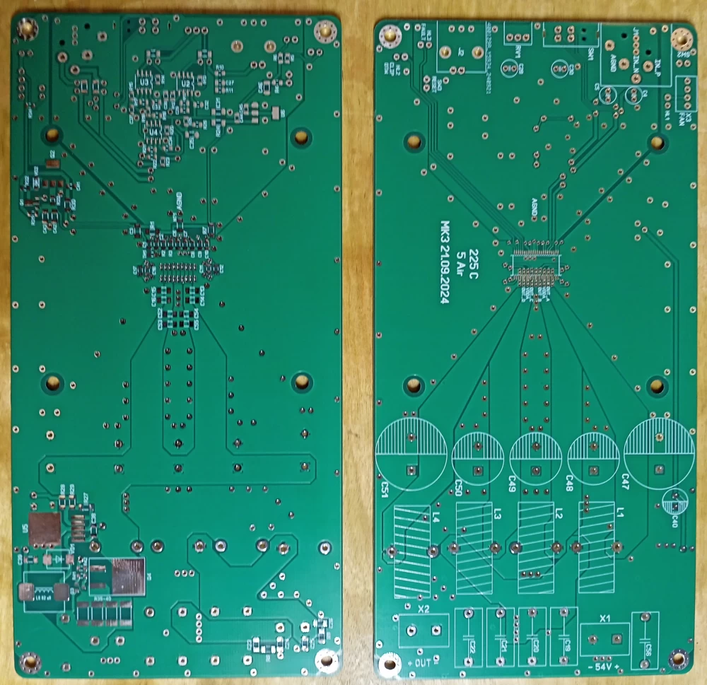
The printed circuit board, taking into account all the changes, I made in Sprint Layout. The board uses FR-4 fiberglass with a copper layer thickness of 2 oz.
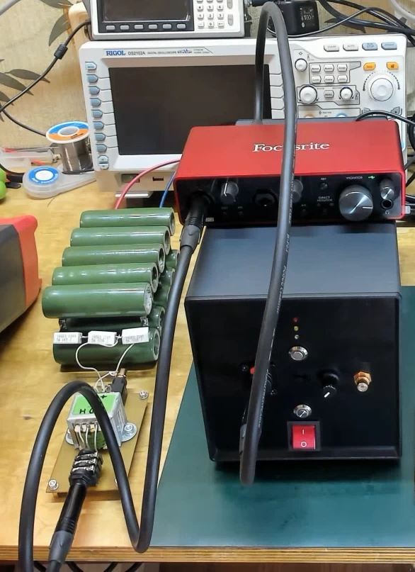
Measurements of the amplifier characteristics using the RMAA program.







Write comment